Speculation: Ryzen 4000 series/Zen 3

Page 28 - Seeking answers? Join the AnandTech community: where nearly half-a-million members share solutions and discuss the latest tech.

jamescox

Senior member
Nov 11, 2009
637
1,103
136
I'm not sure it would (how do they manage DRAM stacking in mobile?). I'm not talking about a whole stack, I'm talking about a single high stack which should remove the need for TSVs as you wouldn't be routing through the HBM (which is what the TSVs are there for). Plus there's possibility that you could implement the HBM in the die itself, and they could segment easily based on the viable amount. I don't believe that the I/O die gains a lot from being shrunk, and to me HBM3 using the same process provides an opportunity that I think would be very beneficial to take advantage of.

I'm talking about in an APU itself. There's quite a few companies that don't want to bother with an extra chip (GPU), but they're fairly constrained by memory bandwidth with regards to GPU performance in current APUs. Which as they move to chiplets the distinction there becomes a bit semantic, but for the OEM it would be a single chip solution, and its something they could do without needing to overhaul the work they did on the substrate for Zen 2 - which they talked up how much work they did there.


By Keller's own words he's there to develop next gen interconnect (which I believe he talked about one that could scale up from intrachip to interchip, and then even system - i.e. unified memory/storage that leverages different tiers trying to make that transparent to the system - and network/datacenter; that to me sounds a lot like the talk about moving to fiber optic, which he's likely looking at is it time to start that transition or can they push the limits of metal first). The way he talked he doesn't seem to have anything to do with the core designs (architecture, etc). Seems that he's there to get the various chips communicating in an efficient and fast manner (which will be needed with move to chiplet designs and co-processing and other things).

Which, I think that's what he was working on at Tesla, is figuring out how to get all the various components (sensors, processing) communicating, while trying to cut down the wiring (for weight, complexity, and cost reasons), but push latency down and throughput up.

And I think there was talk that actually was kinda his focus with Zen (basically InfinityFabric and designing chips to utilize that). I might be very wrong though, but I do know he himself said he's at Intel for developing interconnect.

So, how exactly would the HBM connect to the IO die it is stacked on without having TSVs in the IO die, making it equivalent to an active interposer?p For low performance stuff (like mobile or NAND flash die), they sometimes do stacking by just offsetting the chips and using essentially little wires attached to the edge of the chips (similar to old style wire bonding). That might be fine for a DDR channel or NAND interface, but not for a 1024-bit HBM bus.
 

jamescox

Senior member
Nov 11, 2009
637
1,103
136
Depends on the customer, and their priority use cases.

Given the heavy use of SIMD in software video encoders, you can bet that Google, Netflix, Twitch, Vimeo and anyone else heavily reliant on video platforms will eye any increases in SIMD performance very closely.
Depends on the customer, and their priority use cases.

Given the heavy use of SIMD in software video encoders, you can bet that Google, Netflix, Twitch, Vimeo and anyone else heavily reliant on video platforms will eye any increases in SIMD performance very closely.

Do any of them that aren’t streaming live (like twitch) actually re-encode on the fly? I would expect most videos would get uploaded and encoded to a set of formats and bit rates once. That would then be distributed to a huge network of storage servers and never re-encoded again. Storage servers don’t really need FP at all. In fact, they don’t need much compute performance at all. The Xeon-D parts are kind of made for storage servers with 4 integrated 10 GBit Ethernet. They also are low clock parts, only around 2 GHz.

I don’t have time to look it up now, but I am pretty sure that I have heard of at least google using special hardware encoders. A hardware encoder will generally beat any general purpose solution in performance and power consumption. Perhaps not quality though. Live streaming isn’t generally that great of quality, so I would wonder how many of them are using hardware encoders rather than cpu with software encoders.

AVX512 is a complete wast of die area for a large number of servers. It will mostly be used in HPC machines which is a separate market from the general server market. HPC machines can have all different requirements for different components. I work with some machines that are essentially running HPC applications, but the AVX units in the cpu are completely unused since it is just processing data to pass to the gpus for the real work.

In my opinion, AVX512 was Intel’s attempt to make a cpu perform like a gpu. It doesn’t seem to have worked that well; intel has given in and is now designing an actual gpu. A gpu will probably still outperform AVX512 at better power consumption if the software is updated to use gpus. I would expect that AVX512 is mostly unused except for HPC applications and a few niche consumer and professional apps. Once intel has a high performance gpu, I would wonder how much use AVX512 will actually get.
 

soresu

Platinum Member
Dec 19, 2014
2,676
1,887
136
Do any of them that aren’t streaming live (like twitch) actually re-encode on the fly?

Your post is formatted wrong somewhere - you double quoted me and your own comment is framed within my quote.

I can't think of any reason to waste server time doing such a thing for pre-recorded video.

Obviously for something like Stadia, on-the -fly is a necessity for Google, but as you say that is live.

Any pre-recorded video will be uploaded, re-encoded to several different resolutions at upload time (or ASAP given current server hardware occupancy), and then stored on a server for distribution.

I do agree that 512 bit vector SIMD is getting a bit ridiculous, but CPU's and GPU's are different beasts - modern CPU's support heavy branching code that brings GPU performance screeching to a slow burn.

I'm not sure how difficult it would be to sort such a situation, short of using a compiler to shunt the branch heavy code to the CPU, and the data throughput code/data to the GPU.

Though at that point it starts to sound more like HSA/HSAIL from AMD - they couldn't push it then, I doubt they can now however much market share they claw back.
 

Ajay

Lifer
Jan 8, 2001
15,482
7,883
136
I'm not sure how difficult it would be to sort such a situation, short of using a compiler to shunt the branch heavy code to the CPU, and the data throughput code/data to the GPU.

it’s not the compiler's job. A developer optimizes the data on the cpu and then copies it over to GPU (optimizations like coalescing). The GPU 'kernel' code then executes a series of operations on the data which is then copied back to the systems main memory. So, yes, all the branchy code would execute on the cpu; the biggest issue is actual data transfer rates between cpu/main memory and the GPU. Well, in a nutshell.
 

soresu

Platinum Member
Dec 19, 2014
2,676
1,887
136
it’s not the compiler's job. A developer optimizes the data on the cpu and then copies it over to GPU (optimizations like coalescing). The GPU 'kernel' code then executes a series of operations on the data which is then copied back to the systems main memory. So, yes, all the branchy code would execute on the cpu; the biggest issue is actual data transfer rates between cpu/main memory and the GPU. Well, in a nutshell.
So, direct IF between dies on the package/SoC then?

A unified memory pool was part of the whole HSA ideal - with HBM on the package that would finally be realised in a fairly compact low latency manner.

Even better still in a fully vertically integrated stack (though obviously thermal constraints require creative ICEcool like solutions to keep it from burning up).
 

Thunder 57

Platinum Member
Aug 19, 2007
2,676
3,802
136
New uarch Zen 3, new 19h Family number..... and the main improvement is just unified L3 cache? It looks like fake.
Zen 2 was still 17h Family and brought pretty big changes, new L1 cache, adding 1 store unit, doubling FPU performance.

I can't beleive new uarch with new 19 Family number will bring smaller improvements than Zen 2. This doesn't make sense performance wise. How much can bring that unified L3 cache? 2-4% in average? Is it worth of effort for such a tine change to port Zen2 CPU at completely different EUV process node? For this small change I would expect to stay at N7 non-EUV process, or go to N7P or N6.

I would expect from 19h Family at least new instructions set support (AVX512), so new FPUs, effectivelly doubling the FPU performace as Zen 2 did. Zen3 team is lead by Zen1 architect, so ....

It's not fake, lol. Biggest improvement is unified L3 cache? How about moving from four core CCX to eight? That's a big undertaking, and should pay dividends. No more cross-CCX latency penalty. Besides, what don't know what else they may do. AMD may add AVX 512 support, but not with 512 bit vectors. Too much die cost. I could see them doing 256 x 2 like they did 128 x 2 for Zen(+). They are probably going wider (6 ALU / 4 AGU?). A name change does not have to mean much. K10 was little more than K8 with 128 bit SSE, some cache redesign, and a few small other things perhaps.

So, direct IF between dies on the package/SoC then?

A unified memory pool was part of the whole HSA ideal - with HBM on the package that would finally be realised in a fairly compact low latency manner.

Even better still in a fully vertically integrated stack (though obviously thermal constraints require creative ICEcool like solutions to keep it from burning up).

I'd really like to see another attempt to push HSA. Even Anand said in the review of Kaveri(?) that it was "a big deal". The problem then was AMD had lackluster CPU's and little market share. It would be interesting to see what they could do with it now.
 

LightningZ71

Golden Member
Mar 10, 2017
1,628
1,898
136
Remember, APUs at AMD are NOT premium products and not on leading edge nodes. With that said, Renoir is likely STILL a four core APU, using the same zen 2 CCX as Milan does, likely also with 16MB of L3 this time, using N7 still, and using the same VEGA CUs as Vega VII does. It will have one new piece from AMD, an updated memory controller, likely the one from Milan, but ported over to the N7 process. This has a slim chance of gaining support for lpddr4x.

The 5000 series APUs will likely be the first APUs from AMD that have more than four cores. I suspect that, at N7+, they will use a six core zen 3 CCX with a 24MB L3 and with 12-14 NAVI CUs, with a slightly improved memory controller (likely AMDs first LP-DDR4x controller).

I do see a business opportunity for AMD with GloFo's 12nm+ product. AMD could remask the 3000 series APUs for 12+ and take advantage of the density improvements and power improvements to make a low cost Athlon series for the bottom end of the stack. In almost any iteration, they would be miles better than any of Intel's atom processors that are currently known to be on the drawing board.
 

Ajay

Lifer
Jan 8, 2001
15,482
7,883
136
So, direct IF between dies on the package/SoC then?

A unified memory pool was part of the whole HSA ideal - with HBM on the package that would finally be realised in a fairly compact low latency manner.

Even better still in a fully vertically integrated stack (though obviously thermal constraints require creative ICEcool like solutions to keep it from burning up).

I may be off track here (it's late), but, for example, in an HPC configuration GPUs are connected to the motherboard via a mezzanine connector for maximum performance. Using NVLink 2.0, a GV100 SMX2 can hit peak transfers of 150 GBytes/sec bidirectionally (using 6 sublinks x 25 GB/sec). That's the bandwidth range that's needed. I don't know how this is configured physically with the CPU and system memory to reach those kind of speeds (maybe it's only burst rates from GPU to GPU). How does one achieve this with AMD IF links - I surely do not know.
 

soresu

Platinum Member
Dec 19, 2014
2,676
1,887
136
I may be off track here (it's late), but, for example, in an HPC configuration GPUs are connected to the motherboard via a mezzanine connector for maximum performance. Using NVLink 2.0, a GV100 SMX2 can hit peak transfers of 150 GBytes/sec bidirectionally (using 6 sublinks x 25 GB/sec). That's the bandwidth range that's needed. I don't know how this is configured physically with the CPU and system memory to reach those kind of speeds (maybe it's only burst rates from GPU to GPU). How does one achieve this with AMD IF links - I surely do not know.
PCIe 5.0 spec has superior bandwidth to NVLink 2.0 - I doubt bandwidth requirements will increase that dramatically in the 2 years it will take for 5.0 to make it into products + CXL of course which is based on it.

Theres also Gen-Z too - v1.1 spec was just announced on friday, link here.
 

Ajay

Lifer
Jan 8, 2001
15,482
7,883
136
PCIe 5.0 spec has superior bandwidth to NVLink 2.0 - I doubt bandwidth requirements will increase that dramatically in the 2 years it will take for 5.0 to make it into products + CXL of course which is based on it.

Theres also Gen-Z too - v1.1 spec was just announced on friday, link here.
Well, we'll see if GenZ goes anywhere.
PCIe 5.0 - >
Wikipedia said:
Bandwidth was expected to increase to 32 GT/s, yielding 63 GB/s in each direction in a 16 lane configuration.

So, still less than the max supported by NVLink 2.0, but much better than than earlier versions. I don't know what the latency differences are between the two specs.
Anyway, I imagine Nvidia will have some proprietary NVLinke 3.0 or the like by the time PCIe 5.0 arrives - they aren't known for sitting on their hands. So far, AMD's targeting Cloud Services, etc. rather than HPC. Also, NV doesn't have it's own CPU.

I suppose the bottom line is some converged ultra high performance interconnect between CPU, RAM and GPU are needed for HPC/ML going forward and AMD has work to do when it decides to branch into that market.

All IMHO.
 

soresu

Platinum Member
Dec 19, 2014
2,676
1,887
136
So, still less than the max supported by NVLink 2.0, but much better than than earlier versions. I don't know what the latency differences are between the two specs.
Not sure how the Wikipedia page got to that 63 GB/s number:
1570337322486.png

Also found this quote on the architecture page about Zen2 on Techpowerup:

"Infinity Fabric is the interconnect that binds the three dies by providing a 100 GB/s data path between each CPU chiplet and the I/O controller"
 
Last edited:
  • Like
Reactions: amd6502

jamescox

Senior member
Nov 11, 2009
637
1,103
136
Remember, APUs at AMD are NOT premium products and not on leading edge nodes. With that said, Renoir is likely STILL a four core APU, using the same zen 2 CCX as Milan does, likely also with 16MB of L3 this time, using N7 still, and using the same VEGA CUs as Vega VII does. It will have one new piece from AMD, an updated memory controller, likely the one from Milan, but ported over to the N7 process. This has a slim chance of gaining support for lpddr4x.

The 5000 series APUs will likely be the first APUs from AMD that have more than four cores. I suspect that, at N7+, they will use a six core zen 3 CCX with a 24MB L3 and with 12-14 NAVI CUs, with a slightly improved memory controller (likely AMDs first LP-DDR4x controller).

I do see a business opportunity for AMD with GloFo's 12nm+ product. AMD could remask the 3000 series APUs for 12+ and take advantage of the density improvements and power improvements to make a low cost Athlon series for the bottom end of the stack. In almost any iteration, they would be miles better than any of Intel's atom processors that are currently known to be on the drawing board.

Am I missing something? Milan is zen 3 based Epyc with, apparently, an 8 core CCX. They are having the APU a generation behind the cores for other markets. I would expect Ryzen 4000 APUs to be Zen 2 based with 8 cores in 2 four core CCX, same as current Zen 2 based parts. The zen 3 based desktop, workstation, and server parts will come a bit later. They have doubled the core count for most of their other products from Zen 1 to Zen 2, so I done know why mobile would be any different.
 

NostaSeronx

Diamond Member
Sep 18, 2011
3,687
1,222
136
A name change does not have to mean much. K10 was little more than K8 with 128 bit SSE, some cache redesign, and a few small other things perhaps.
K7, K8, Hound, Husky cores are all the same family; Family 00h w/ loose model/family interoperability: 07h for K7, 0Fh for K8, and Hound is 10h, Husky is 12h, etc. There are K7 cores in K8's numbers as 0Fh and K8 cores in Hound's numbers as 11h.

Changes from the above from 14h/15h onward are maintained in a single family with AMD. A dramatic shift or change in architecture comes with a new Family number.
 
Last edited:

jamescox

Senior member
Nov 11, 2009
637
1,103
136
Not sure how the Wikipedia page got to that 63 GB/s number:
View attachment 11657

Also found this quote on the architecture page about Zen2 on Techpowerup:

"Infinity Fabric is the interconnect that binds the three dies by providing a 100 GB/s data path between each CPU chiplet and the I/O controller"

I believe that is due to the 128b/130b coding. The embedded clock reduces the actual max transfer rate slightly. Pci-express 2.0 used 8b/10b coding so the actual max bandwidth was reduced more than with 3.0 and 4.0. I think infinity fabric in Zen 2 is actually 25 GT/s, so it is faster than pci-express 4.0, but slower than 5.0; about 50 GB/s. It can transfer in both directions simultaneously, so it is near 100 GB/s aggregate.

Epyc IO capabilities are ridiculous. A single 4.0 link is 1.969 GB/s. For 128 links that is over 252 GB/s in each direction. DDR4-3200 is 25.6 GB/s per channel, so Epyc with 8 channels is 204.8 GB/s. It has more raw IO bandwidth than the memory bandwidth.
 

jamescox

Senior member
Nov 11, 2009
637
1,103
136
Well, we'll see if GenZ goes anywhere.
PCIe 5.0 - >

So, still less than the max supported by NVLink 2.0, but much better than than earlier versions. I don't know what the latency differences are between the two specs.
Anyway, I imagine Nvidia will have some proprietary NVLinke 3.0 or the like by the time PCIe 5.0 arrives - they aren't known for sitting on their hands. So far, AMD's targeting Cloud Services, etc. rather than HPC. Also, NV doesn't have it's own CPU.

I suppose the bottom line is some converged ultra high performance interconnect between CPU, RAM and GPU are needed for HPC/ML going forward and AMD has work to do when it decides to branch into that market.

All IMHO.

Infinity fabric is roughly the same speed as nvlink 2.0, if I am reading the specs correctly. They both operate at 25 GT/s; faster than pci-express 4.0, but slower than 5.0. That is about 50 GB/s in each direction for an x16 link.
 

Richie Rich

Senior member
Jul 28, 2019
470
229
76
Here is my topology sketch, updated for Milan with the the 8-core CCX. Note that the L4 blocks may just be cache-coherency directory slices, but could conceivably include last-level cache. Note that cores/L3 slices are interconnected using the same topology as the L4 slices.

View attachment 11630

Here is this topology illustrated on the current package design used for Rome:

View attachment 11631
Just technical note:
- 4 CPU CCX = mesh with 6 interconnections
- 8 CPU CCX = mesh with 28 interconnectons (5 times more complicated and slower)

That's why AMD uses 4c CCX, it's simple and fast. If they want to unify L3 cache they would have to use ring-bus like Intel IMHO.
 
  • Like
Reactions: Kirito and Vattila

DisEnchantment

Golden Member
Mar 3, 2017
1,615
5,861
136
Quoting myself here

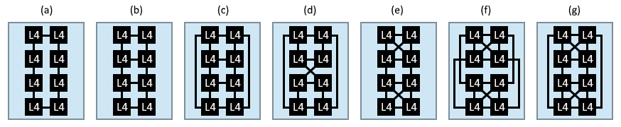
- 8 Core CCX (Also mentioned by S|A, patent drawings indicate so but it is exemplary)
- Single L3 in one CCX (from #20180239708, #20180143829, #20180165202) same as Zen 1
- Memory Controller located in another chiplet connected by an interconnect (called bridge chiplet by AMD) (from #20180239708, #20180143829, #20180165202)
- Data compression across IF (from Patents see #20180167082 (across sockets) and #20180052631 (across dies)) not in Zen 1. If compressed data is lesser than bus width the extra bits are not even signalled. (#20180314655)
- Directory Controller for L3 sync across dies ( from Patents see #20180239708) which is not the case in Zen 1
- According to David Schor/gcc patches Load/Store costs for(>=256 bit SSE) are halved. I don't know if it is definitive but this is a significant improvement.
- Many improvements related to cache if Patents are to be believed. Something like 8-10 patents in last year.

Those patent applications were for real after all.

I add some new ones below , cache related only:p

20190179758 CACHE TO CACHE DATA TRANSFER ACCELERATION TECHNIQUES
Systems, apparatuses, and methods for accelerating cache to cache data transfers are disclosed. A system includes at least a plurality of processing nodes and prediction units, an interconnect fabric, and a memory. A first prediction unit is configured to receive memory requests generated by a first processing node as the requests traverse the interconnect fabric on the path to memory. When the first prediction unit receives a memory request, the first prediction unit generates a prediction of whether data targeted by the request is cached by another processing node. The first prediction unit is configured to cause a speculative probe to be sent to a second processing node responsive to predicting that the data targeted by the memory request is cached by the second processing node. The speculative probe accelerates the retrieval of the data from the second processing node if the prediction is correct.

20190179760 CACHE CONTROL AWARE MEMORY CONTROLLER
Systems, apparatuses, and methods for accelerating cache to cache data transfers are disclosed. A system includes at least a plurality of processing nodes and prediction units, an interconnect fabric, and a memory. A first prediction unit is configured to receive memory requests generated by a first processing node as the requests traverse the interconnect fabric on the path to memory. When the first prediction unit receives a memory request, the first prediction unit generates a prediction of whether data targeted by the request is cached by another processing node. The first prediction unit is configured to cause a speculative probe to be sent to a second processing node responsive to predicting that the data targeted by the memory request is cached by the second processing node. The speculative probe accelerates the retrieval of the data from the second processing node if the prediction is correct.

20190095330 PREEMPTIVE CACHE WRITEBACK WITH TRANSACTION SUPPORT
A method of preemptive cache writeback includes transmitting, from a first cache controller of a first cache to a second cache controller of a second cache, an unused bandwidth message representing an unused bandwidth between the first cache and the second cache during a first cycle. During a second cycle, a cache line containing dirty data is preemptively written back from the second cache to the first cache based on the unused bandwidth message. Further, the cache line in the second cache is written over in response to a cache miss to the second cache

20190108154 METHOD AND APPARATUS FOR POWER REDUCTION FOR DATA MOVEMENT
A method of and device for transferring data is provided. The method includes determining a difference between a data segment that was transferred last relative to each of one or more data segments available to be transferred next. In some embodiments, for so long as no data segment available to be sent has been waiting too long, the data segment chosen to be sent next is the data segment having the smallest difference relative to the data segment transferred last. The chosen data segment is then transmitted as the next data segment transferred.

20190188137 REGION BASED DIRECTORY SCHEME TO ADAPT TO LARGE CACHE SIZES
Systems, apparatuses, and methods for maintaining a region-based cache directory are disclosed. A system includes multiple processing nodes, with each processing node including a cache subsystem. The system also includes a cache directory to help manage cache coherency among the different cache subsystems of the system. In order to reduce the number of entries in the cache directory, the cache directory tracks coherency on a region basis rather than on a cache line basis, wherein a region includes multiple cache lines. Accordingly, the system includes a region-based cache directory to track regions which have at least one cache line cached in any cache subsystem in the system. The cache directory includes a reference count in each entry to track the aggregate number of cache lines that are cached per region. If a reference count of a given entry goes to zero, the cache directory reclaims the given entry.

20190196974 TAG ACCELERATOR FOR LOW LATENCY DRAM CACHE
Systems, apparatuses, and methods for implementing a tag accelerator cache are disclosed. A system includes at least a data cache and a control unit coupled to the data cache via a memory controller. The control unit includes a tag accelerator cache (TAC) for caching tag blocks fetched from the data cache. The data cache is organized such that multiple tags are retrieved in a single access. This allows hiding the tag latency penalty for future accesses to neighboring tags and improves cache bandwidth. When a tag block is fetched from the data cache, the tag block is cached in the TAC. Memory requests received by the control unit first lookup the TAC before being forwarded to the data cache. Due to the presence of spatial locality in applications, the TAC can filter out a large percentage of tag accesses to the data cache, resulting in latency and bandwidth savings.

20190163632 REDUCING CACHE FOOTPRINT IN CACHE COHERENCE DIRECTORY
A method includes monitoring, at a cache coherence directory, states of cachelines stored in a cache hierarchy of a data processing system using a plurality of entries of the cache coherence directory. Each entry of the cache coherence directory is associated with a corresponding cache page of a plurality of cache pages, and each cache page representing a corresponding set of contiguous cachelines. The method further includes selectively evicting cachelines from a first cache of the cache hierarchy based on cacheline utilization densities of cache pages represented by the corresponding entries of the plurality of entries of the cache coherence directory.
 

Tuna-Fish

Golden Member
Mar 4, 2011
1,357
1,564
136
Just technical note:
- 4 CPU CCX = mesh with 6 interconnections
- 8 CPU CCX = mesh with 28 interconnectons (5 times more complicated and slower)

That's why AMD uses 4c CCX, it's simple and fast. If they want to unify L3 cache they would have to use ring-bus like Intel IMHO.

As I have pointed out many times, this is not correct. Cores are not attached to each other, they are attached to cache. 4CPU CCX has 16 interconnections, from each core to each slice of cache.

And cache topology does not need to match the topology of cores. Right now, the L3 slices serve halves of cache lines per cycle. If that is doubled to a full cache line, they maintain the same throughput per core, even if they only use 4 slices, allowing them to use 8*4=32 interconnections, or the same count as the sum of the interconnections in two CCX:es.
 

NTMBK

Lifer
Nov 14, 2011
10,241
5,031
136
I didn't see the video before it was taken down. Did it confirm SMT2?
 

Vattila

Senior member
Oct 22, 2004
799
1,351
136
If they want to unify L3 cache they would have to use ring-bus like Intel IMHO.

That would be a big redesign. Also, a ring topology has its flaws — in particular it has many hops (large diameter) and suffers from contention. A cube topology (g) seems to me the easiest to implement based on the existing 4-core CCX. See the CCX thread for a discussion of topologies. From a subsequent post of mine:

"Each L3 slice only needs another connection port to connect to the corresponding slice in the other 4-core group. I presume that the low-level interconnects between cache slices in the 4-core groups and between groups are of the same kind, to optimise uniformity in latency."

9114301_0f212bd248718fe6fee76dc051801709.png


(Note: Replace L4 by L3 in these diagrams.)
 
Last edited:
  • Like
Reactions: Kirito

Vattila

Senior member
Oct 22, 2004
799
1,351
136
As I have pointed out many times, this is not correct. Cores are not attached to each other, they are attached to cache. 4CPU CCX has 16 interconnections, from each core to each slice of cache.

I am confused. As I understand it, cores are, as you say, directly attached to their L3 slice. However, the 4 slices in the current CCX are fully connected with 6 bidirectional links. I haven't seen this number 16 claimed anywhere else. Can you draw a diagram to explain what you mean? See my topology discussion for reference.
 
Last edited: