All things going to plan We will see zen3 in 2020 because a super computer is using it.
No, that's a custom CPU. One would think it borrows heavily from Zen2/3 but AMD has said yet AFAIK.

All things going to plan We will see zen3 in 2020 because a super computer is using it.
http://www.chip-architect.com/news/2001_10_02_Hammer_microarchitecture.htmlI would like to know what was the spec of Keller's K8 prototype, but I cannot find it anywhere.
No im not talking about the frontier super computer im talking milian in Perlmutter which is late 2020.No, that's a custom CPU. One would think it borrows heavily from Zen2/3 but AMD has said yet AFAIK.
I wouldn't assume that, you need to clock this thing, how many read/write ports are you going to have to your PRF? How are you going to handle load and store bandwidth, cache configuration. How are you going to get enough decode bandwidth? There are limited use cases where SMT4 can make sense otherwise your just dividing your resources by 4 and in physics things dont scale linearly so you will loose clocks big time if you scale out all those structures, especially anything that needs to read and write.Assuming Zen3 is wider (6xALU, SMT4) core..... then 8core Zen3 chiplet area will be similar to 12c Zen2 area. I think they can keep well proofed quad-core CCX still.
doubt it . 7nm+ gives a ~20% density improvement, use that 20% to drive perf per clock up 10-20%, increase CCD's to ~ 100mm, 96 cores , 192 thread EPYC 3. Will be much better for almost all markets (especially the high volume server markets) then 64C/256T chip.Zen3 8c/32t chiplet might be +50% bigger in area/transistors/power consump, +70% in overall performance. This could be tight to fit 64c under heat-spreader.
Who the heck started this SMT4 rumor?Assuming Zen3 is wider (6xALU, SMT4) core
No idea but it's very stupid.Who the heck started this SMT4 rumor?
I want to say it was our friendly neighborhood cat prophet, but I don't know for sure.
Edit: Yep, I was right. Seems to originate all the way back over 2 years ago starting with this post. However, he was talking about his mythical low power follow-up to AMD's cat line of CPUs but obviously that didn't pan out but it got the talk going about SMT4 capable AMD CPUs.
Later it is mentioned in passing here speculating on what Zen2 would look like. Responses basically saying it would be interesting to see but was doubtful. Small group of posters continue to speculate about SMT4 being in Zen2. Since that didn't pan out either the speculation about SMT4 being designed into an AMD architecture shifted to Zen3 starting with this post here.
I wouldn't assume that, you need to clock this thing, how many read/write ports are you going to have to your PRF? How are you going to handle load and store bandwidth, cache configuration. How are you going to get enough decode bandwidth? There are limited use cases where SMT4 can make sense otherwise your just dividing your resources by 4 and in physics things dont scale linearly so you will loose clocks big time if you scale out all those structures, especially anything that needs to read and write.
doubt it . 7nm+ gives a ~20% density improvement, use that 20% to drive perf per clock up 10-20%, increase CCD's to ~ 100mm, 96 cores , 192 thread EPYC 3. Will be much better for almost all markets (especially the high volume server markets) then 64C/256T chip.
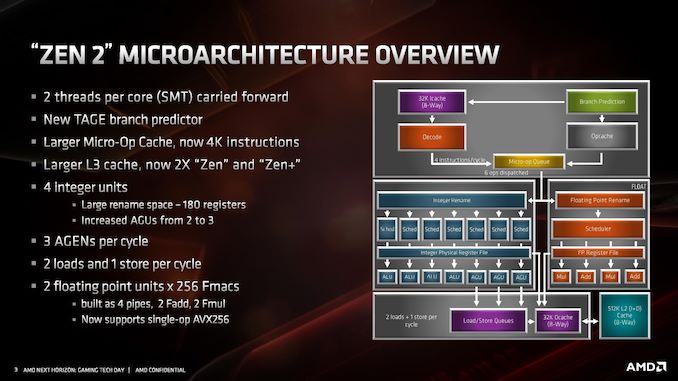
The decoders in Zen 2 stay the same, we still have access to four complex decoders (compared to Intel’s 1 complex + 4 simple decoders), and decoded instructions are cached into the micro-op cache as well as dispatched into the micro-op queue.
AMD has also stated that it has improved its micro-op fusion algorithm, although did not go into detail as to how this affects performance. Current micro-op fusion conversion is already pretty good, so it would be interesting to see what AMD have done here. Compared to Zen and Zen+, based on the support for AVX2, it does mean that the decoder doesn’t need to crack an AVX2 instruction into two micro-ops: AVX2 is now a single micro-op through the pipeline.
Going beyond the decoders, the micro-op queue and dispatch can feed six micro-ops per cycle into the schedulers. This is slightly imbalanced however, as AMD has independent integer and floating point schedulers: the integer scheduler can accept six micro-ops per cycle, whereas the floating point scheduler can only accept four. The dispatch can simultaneously send micro-ops to both at the same time however.
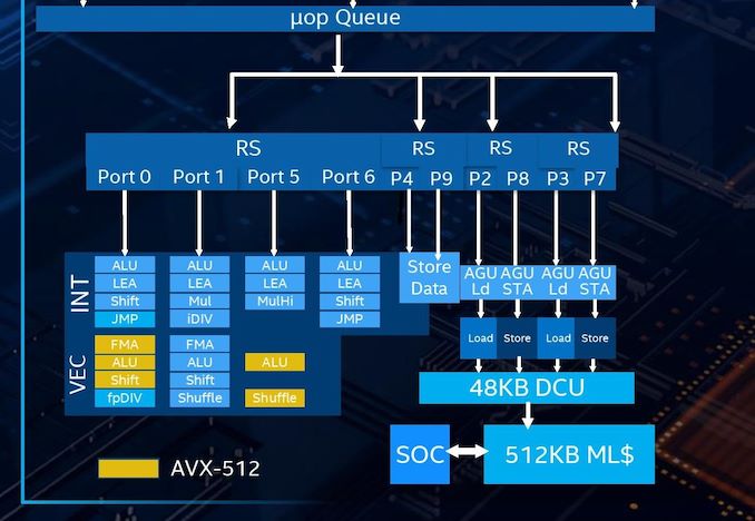
The micro-op cache gets an update here, from 1.5k entries to 2.25k entries. This is the first time that Intel has increased the micro-op cache size since Haswell, but it should be noted that the competition also has micro-op caches (ARM has 1.5k, AMD has 2k for Zen, 4k for Zen 2), and so refinement in this area is going to be critical. The micro-op cache can supply six micro-ops to the queue per cycle.
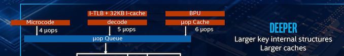
Overall, six micro-ops can be fed between the decoders/cache/direct micro-code per cycle. That is split between up to six per cycle from the cache, up to 5 from the decoders, and up to 4 from direct microcode (which gets fed through the complex decoder).
In total, the number of execution ports has increased from 8 in Skylake to 10 in Sunny Cove. This allows for 10 micro-ops per cycle to be dispatched from the reorder buffer, a 25% increase. The two new ports lie in different areas: Skylake had 3 AGUs, supporting two loads and one store per cycle, but Sunny Cove now has 4 AGUs, for two loads and two stores per cycle. The other new port is a store data port. With these changes, the L1 data cache can now support two stores per cycle, effectively doubling the L1 store bandwidth.
There's a rumor out there that EPYC 3 will use 14+1 chiplets vs. the current 8+1. Assuming more chiplets can't fit onto the current package without shrinking each chiplet, that implies that the transistor count for each CCD can't increase too much over EPYC 2 or else the chiplet size doesn't decrease. If the transistor budget can't increase, I'm not sure how likely it is to extract a whole lot of IPC gains in Zen 3, but this is just a theory.
its already been confirmed by AMD Zen3 is DDR4.Unless they choose to go DDR5 since the decoupled memory controller allows to differentiate between desktop and server, and have a new socket for server only.
Forrest Norrod: DDR5 is a different design. It will be on a different socket. We've already said Milan is a mid-2020 platform, and we've already said that's socket SP3, so DDR4 will still be used for Milan.
Yes and maybe no. There were industry rumors that AMD is looking to beat Intel to DDR5, so that statement might be intentionaly misleading.its already been confirmed by AMD Zen3 is DDR4.
https://www.anandtech.com/show/14568/an-interview-with-amds-forrest-norrod-naples-rome-milan-genoa
Therefore Milan not supporting might not be the same as Zen3 not supporting. I agree I'm reaching a bit, but the possibility is not entirelly outlandish
its already been confirmed by AMD Zen3 is DDR4.
https://www.anandtech.com/show/14568/an-interview-with-amds-forrest-norrod-naples-rome-milan-genoa
Well you dont just dump a 6 cyl engine in a platform made for 4 cyl. You need to beef up the rest.What might be a Zen3?
Answer is: what is the inevitable future of CPU cores?
The real power is in back-end and it's ALUs, AGUs and FPUs. As a mech engineer I see these as cylinders in the engine.
Front-end is just feeding them as efficiently as possible. Same as intake manifold is feeding engine. That's all.
The evolution of back-end ALUs was:
- 1995 ... 2xALU Intel P6 uarch, PentiumPro, PII...
- 1997 ... 2xALU AMD/Nexgen K6
- 1999 ... 3xALU AMD K7, Intel PIII
- 2008 ... 4xALU Intel Nehalem
- 2012 ... 4xALU AMD Zen
- 2017 ... 6xALU Apple A11 ... most powerful core today (int IPC +76% over Skylake)
x86 CPUs must move to 6xALUs. When Apple did it then Intel and AMD must do that too. Sure, It will be hard move as was move from 3xALU -> 4xALU, it will need core re-design from scratch, same as Nehalem and Zen were. You don't need to be genius to predict that inevitable future is 8xALUs core design as a next step. Or do you think x86 CPUs will sit at 4xALU design for next 50 years? No. Apple moved from weak 4-cylinder engine to their powerfull V6. However I think we deserve V8s.
What is the evolution of SMT?
- 1999 introduced by DEC in 1999, implemented in CPU EV8 SMT4 in 2003 (cancelled in 2001 by Compaq in favor of Itanium)
- 2002 ... Intel P4 SMT2
- 2004 ... IBM Power5 SMT2
- 2010 ... IBM Power7 SMT4 dynamical
- 2014 ... IBM Power8 SMT8 dynamical
- 2017 ... AMD Zen SMT2
- 2050 ... x86 still stuck at SMT2?
6xALU core still might be fine with SMT2. For high thread server application SMT4 makes sense even for this core.
8xALU core will struggle with just SMT2 from efficiency point. You do not need to be genius to predict that SMT4 for this core is efficient move. SMT4 and SMT8 with dynamical changing number of threads/priority is actual IBM technology, not a sci-fi. Again, you do not need to be genius to predict that next step is SMT-16 (for very wide core and some specific server markets). Does SMT4 still look crazy for Zen3?
And don't forget guys what Kennedy said: "We choose to go to the moon because it is hard, not because it is easy."
What might be a Zen3?
Answer is: what is the inevitable future of CPU cores?
The real power is in back-end and it's ALUs, AGUs and FPUs. As a mech engineer I see these as cylinders in the engine.
Front-end is just feeding them as efficiently as possible. Same as intake manifold is feeding engine. That's all.
The evolution of back-end ALUs was:
- 1995 ... 2xALU Intel P6 uarch, PentiumPro, PII...
- 1997 ... 2xALU AMD/Nexgen K6
- 1999 ... 3xALU AMD K7, Intel PIII
- 2008 ... 4xALU Intel Nehalem
- 2012 ... 4xALU AMD Zen
- 2017 ... 6xALU Apple A11 ... most powerful core today (int IPC +76% over Skylake)
x86 CPUs must move to 6xALUs. When Apple did it then Intel and AMD must do that too. Sure, It will be hard move as was move from 3xALU -> 4xALU, it will need core re-design from scratch, same as Nehalem and Zen were. You don't need to be genius to predict that inevitable future is 8xALUs core design as a next step. Or do you think x86 CPUs will sit at 4xALU design for next 50 years? No. Apple moved from weak 4-cylinder engine to their powerfull V6. However I think we deserve V8s.
What is the evolution of SMT?
- 1999 introduced by DEC in 1999, implemented in CPU EV8 SMT4 in 2003 (cancelled in 2001 by Compaq in favor of Itanium)
- 2002 ... Intel P4 SMT2
- 2004 ... IBM Power5 SMT2
- 2010 ... IBM Power7 SMT4 dynamical
- 2014 ... IBM Power8 SMT8 dynamical
- 2017 ... AMD Zen SMT2
- 2050 ... x86 still stuck at SMT2?
6xALU core still might be fine with SMT2. For high thread server application SMT4 makes sense even for this core.
8xALU core will struggle with just SMT2 from efficiency point. You do not need to be genius to predict that SMT4 for this core is efficient move. SMT4 and SMT8 with dynamical changing number of threads/priority is actual IBM technology, not a sci-fi. Again, you do not need to be genius to predict that next step is SMT-16 (for very wide core and some specific server markets). Does SMT4 still look crazy for Zen3?
And don't forget guys what Kennedy said: "We choose to go to the moon because it is hard, not because it is easy."
That's why I wrote that wider 6-8xALU core will need re-design from scratch, back-end, front-end, everything. Same they did with Zen, what's the problem? Will their brains hurt during development of this? Yes. Will it take longer to develop that just refurbishing 4xALU core. Yes. But don't forget you cannot develop 4xALU design forever because fruits are higher and higher to reach. There is a limit beyond it's easier to pick 6xALU fruit. It looks like Apple engineers discovered it first.Well you dont just dump a 6 cyl engine in a platform made for 4 cyl. You need to beef up the rest.
As desktop enthusiast we want wider stuff. Is there mm2 for 6x alu design in the current socket 7nm+ ?
They need that big L3 to hide latencies between the CCD and IOD.However instead of doubling L3 cache, which brings few % performance and wasting a lot transistors, they can use it more efficiently.
Interestingly, TSMC announced N7P
Wikichip said:N7P
TSMC has started rolling out an optimized version of their N7 process called N7 Performance-enhanced version (N7P). This process goes by various other names such as “2nd generation 7 nm” and “7 nm year 2”. This process should not be confused with N7+. N7P is an optimized, DUV-based, process which uses the same design rules and is fully IP-compatible with N7. N7P introduces FEOL and MOL optimizations which are said to translate to either 7% performance improvement at iso-power or up to 10% lower power at iso-speed.
Interestingly, TSMC announced N7P. I wonder if this could go in some of the later Ryzen 3k SKUs? Or is this already what is being used in the Ryzen 3k?
N7+ will be a long node for AMD, all the consoles will also be on it.
Ask David Schor on Twitter.What is the view here on that?
No, it has at least relaxed CPP (like 64 vs 54 for mobile).Is the HPC variant just an alternative standard cell library with bigger cells
