Speculation: Ryzen 3000 series

Page 41 - Seeking answers? Join the AnandTech community: where nearly half-a-million members share solutions and discuss the latest tech.

What will Ryzen 3000 for AM4 look like?


  • Total voters
    230

Shivansps

Diamond Member
Sep 11, 2013
3,855
1,518
136
I guess, but apparently it would be noticed by viewers if they pointed it at a camera?
Maybe not but you can bet someone would had noticed if they took a close picture like the one anandtech took of the front side.

Still makes no sense to me to have a non-am4 CPU no show to the press.
 

Markfw

Moderator Emeritus, Elite Member
May 16, 2002
25,554
14,510
136
Now I'm really curious why the desktop IOC is bigger than a quarter of the server IOC. On Zeppelin the uncore was mostly unlocked only in Epyc parts for server while Ryzen used far less of it.
If the same part also supports 16 cores, then that would be half the server, maybe a little less due to 2 channel memory instead of 8.
 
  • Like
Reactions: beginner99

Shivansps

Diamond Member
Sep 11, 2013
3,855
1,518
136
Now I'm really curious why the desktop IOC is bigger than a quarter of the server IOC. On Zeppelin the uncore was mostly unlocked only in Epyc parts for server while Ryzen used far less of it.

yeah its tecnically a NB and IGPs started existing because they wanted to use the empty space on the NB because its a lot of I/O and no so much of anything else.

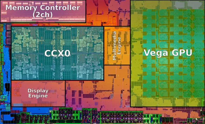
It is really a good question, 2400G die size is 209.73mm and the I/O die is 122.63 mm, the I/O die is only 87mm smaller than this...
800px-raven_ridge_die_%28annotated%29.png


Take away the CCX and the support stuff for it and you are there. Altrought, it probably has L4 inside.
 

Joe Braga

Member
Dec 31, 2017
25
10
51
yeah its tecnically a NB and IGPs started existing because they wanted to use the empty space on the NB because its a lot of I/O and no so much of anything else.

It is really a good question, 2400G die size is 209.73mm and the I/O die is 122.63 mm, the I/O die is only 87mm smaller than this...
800px-raven_ridge_die_%28annotated%29.png


Take away the CCX and the support stuff for it and you are there. Altrought, it probably has L4 inside.
Will it be possible a 7nm Zen2 APU?
 
  • Like
Reactions: AAbattery

Shivansps

Diamond Member
Sep 11, 2013
3,855
1,518
136
Will it be possible a 7nm Zen2 APU?

122mm is a lot for a "NB", if you look at the 2400G all stuff this 122m "I/O" has is at the borders. To me there is SOMETHING in there. And no one asked them about it!
Anyway it probably is L4... but it may be IGP alone, L4 alone or smaller IGP+L4.

Aren't you wondering that is it impossible to exist a R3 3300G and R5 3600G?

Well if the IGP is on the I/O then all Desktop Ryzens are APUs, even the 16C ones. If they want to launch Picasso at desktop and i dont see a reason of why they dont, the 3300G Zen 2 cant exist at $100.
 
  • Like
Reactions: trollspotter

Joe Braga

Member
Dec 31, 2017
25
10
51
122mm is a lot for a "NB", if you look at the 2400G all stuff this 122m "I/O" has is at the borders. To me there is SOMETHING in there. And no one asked them about it!
Anyway it probably is L4... but it may be IGP alone, L4 alone or smaller IGP+L4.


Well if the IGP is on the I/O then all Desktop Ryzens are APUs, even the 16C ones. If they want to launch Picasso at desktop and i dont see a reason of why they dont, the 3300G Zen 2 cant exist at $100.
Why is it impossible? But it couldn't be sold at $119?
 

jpiniero

Lifer
Oct 1, 2010
14,591
5,214
136
Now I'm really curious why the desktop IOC is bigger than a quarter of the server IOC. On Zeppelin the uncore was mostly unlocked only in Epyc parts for server while Ryzen used far less of it.

It's pretty close though, isn't it?

Not so sure about this, but maybe AMD put what would be needed to support Threadripper (eg: quad channel memory and the extra PCIe lanes) on the IO die and both Ryzen and Threadripper share the same IO die.
 

Shivansps

Diamond Member
Sep 11, 2013
3,855
1,518
136
Why is it impossible? But it couldn't be sold at $119?

because they just launched the 240GE at $75, you need to fit Picasso 4/4 and 4/8 SOMEWHERE, there is no room. I do see the 3300G taking 2400G place and the 2400G taking 2200G place.
 

Joe Braga

Member
Dec 31, 2017
25
10
51
They already said NO to GPU chiplets, from were a 3300G is going to come from in six to nine months? Unless that the 3300G is a 4/8 Picasso APU.
I guess that they came back because in their roadmap they done any mention of 12nm+ for Desktop APUs this only be used 12nm+ in Ryzen Mobile APUs lineup
 

moinmoin

Diamond Member
Jun 1, 2017
4,950
7,659
136
If the same part also supports 16 cores, then that would be half the server, maybe a little less due to 2 channel memory instead of 8.
Rome will be up to 64 cores though.

Altrought, it probably has L4 inside.
Why would the desktop IOC get L4$ but the server IOC not? The reverse should be more likely, but doesn't match the size differences. Or both have the same L4$ size.

It's pretty close though, isn't it?
That's my point. Of Zeppelin's uncore there was a lot of IO that wasn't of use on AM4 (even essentially being a quarter of a server). So one would expect the desktop IOC to be clearly smaller than a quarter of the server IOC now that both are distinct designs. The fact that it's close, likely even slightly bigger, combined with the info that there won't be an MCM APU essentially requires that the desktop IOC has some other significant additional stuff the server IOC doesn't.

Not so sure about this, but maybe AMD put what would be needed to support Threadripper (eg: quad channel memory and the extra PCIe lanes) on the IO die and both Ryzen and Threadripper share the same IO die.
I'm expecting Threadripper to use the server IOC. The desktop IOC being prepared for Threadripper would be insane considering it's double the IMC and more than double the PCIe lanes when the Ryzen market dwarfs that of Threadripper. And for Threadripper the IOC would need to be closer to half the server IOC size if a distinct design.
 
Last edited:

amd6502

Senior member
Apr 21, 2017
971
360
136
From AnandTech's article:
View attachment 2314

That's a pretty huge improvement over my R7 1700, at roughly the same chip power...

1421 or so for R7 1700

That's a 44.7% improvement in MT score.

Granted, this is probably the best-case scenario benchmark for them, but with final clocks yet to be decided it will likely only go up between now and release, representing the kind of generational leap we've been missing for a while.

It's great to have competition again.
yeah its tecnically a NB and IGPs started existing because they wanted to use the empty space on the NB because its a lot of I/O and no so much of anything else.

It is really a good question, 2400G die size is 209.73mm and the I/O die is 122.63 mm, the I/O die is only 87mm smaller than this...
800px-raven_ridge_die_%28annotated%29.png


Take away the CCX and the support stuff for it and you are there. Altrought, it probably has L4 inside.

So that's about two CCX's worth of area we're subtracting (or, very approximately the green area and the area below it)

It almost seems like it would leave some room for a small iGPU. A little over a quarter of the green area labeled "Vega" could house 3CU's. The 3CU's and the display engine and MM engine would be about 60% of the green area.


3300g and 3400g (as well as -ge) would logically be 12nm APUs and can be expected launch shortly (~2mo to a quarter) after their mobile packaged counterparts.

Anything 3500 through 3700 might be a mix of 7nm and 12nm (Pinnacles), and anything higher than 3700 I would guess is exclusively 7nm.

Hopefully there will be a 7nm Phenom anniversary release (3c/6t, 4c/8t, and 6c/12t, either or multiple releases).
 
Last edited:
  • Like
Reactions: AAbattery

Shivansps

Diamond Member
Sep 11, 2013
3,855
1,518
136
Removing CCX from the Raven Ridge die also means removing some stuff to support it, that will be also moved to the chiplet, but the fact i can just sustract the CCX size to the RR die size and came out with the same die size an Ryzen 3000 I/O die has is highly suspicious. The Uncore stuff on the I/O die will be minimal if there is no cache or anything. If there is an IGP inside it may be not so small, around Vega 10-11. Then again remember this, if DDR5 is coming in 2020-2021 it is possible that this I/O also have a DDR5 mem controller. The major block would be the physical area for contacts, the number one problem for NBs.
 
Last edited:
  • Like
Reactions: lightmanek

beginner99

Diamond Member
Jun 2, 2009
5,210
1,580
136
Why would the desktop IOC get L4$ but the server IOC not?

Because of latency. It matters more for desktop use especially gaming. Less of an issue in server. Also these 64-core servers will mostly run virtualized environments meaning you will assign cores form the same chiplet to the same VM so no talk between chiplets required and VMs mostly don't need more than 8-cores.

On the other hand this will only benefit the >8 core ryzen parts with more than 1 chiplet. I still think l4 would make sense but it could also be a tiny gpu, 1CU should be more than enough for a windows desktop / 2D + video decode/encode blocks. That would make it more friendly to OEMs. At work I need CPU power not gpu.
 

coercitiv

Diamond Member
Jan 24, 2014
6,199
11,895
136
In all honesty though, an ES running at above 4.0GHz? When was the last time that we saw something like that?
The "problem" with the ES running @ 3.9-4Ghz is the 15%+ increase in IPC over Zen+ in order to get the 2050 CB score. AMD mentioned changes in Zen 2 that are bound to increase IPC by increasing efficiency, which has the "unfortunate" side-effect of decreasing SMT yields, which in turn means that single-threaded IPC increase for CB15 would need to be even higher, say something like 20% to throw a number around.

Personally I would be thrilled if the sample was running at 3.9Ghz and IPC gains were so high, as it's easier to ride 7nm performance improvements and increase clocks rather than wait another cycle for a notoriously hard to get 5-10% jump in IPC.
 

coercitiv

Diamond Member
Jan 24, 2014
6,199
11,895
136
Was there a BD/PD ES clocked that high? Otherwise I can't think of anything from AMD like that.
If we work with previous ES speeds only, then why not be even more bound and consider a 3.6-3.7Ghz sample. That's what... just a 26% IPC jump over Zen+ in a SMT friendly workload. When was the last time Intel achieved a generational jump of 20% in IPC after Haswell?

I also have to wonder, what are the chances that the ES speed AMD would normally work with at this stage happens to match 9900K performance in CB15?
 

DrMrLordX

Lifer
Apr 27, 2000
21,629
10,841
136
If we work with previous ES speeds only, then why not be even more bound and consider a 3.6-3.7Ghz sample. That's what... just a 26% IPC jump over Zen+ in a SMT friendly workload. When was the last time Intel achieved a generational jump of 20% in IPC after Haswell?

I honestly don't know what were the ES speeds for Zen+, but Zen had an ES speed of 3.4 GHz. Zen+ brought ~300 MHz higher turbo limits and 100 MHz higher base clocks (vs 1800x). Not sure if an ES chip will use turbo either. If Zen2 continues the trend on base clocks, the ES should have 3% higher base clock and 8% higher max turbo vs Zen+. That would put Zen2 ES speed at just shy of 3.6 GHz.

I also have to wonder, what are the chances that the ES speed AMD would normally work with at this stage happens to match 9900K performance in CB15?

Pretty low. That performance was most likely for theatrical purposes.
 

naukkis

Senior member
Jun 5, 2002
706
578
136
Now I'm really curious why the desktop IOC is bigger than a quarter of the server IOC. On Zeppelin the uncore was mostly unlocked only in Epyc parts for server while Ryzen used far less of it.

Is it? For me it sure looks just about one quarter of Rome IO-die.

Rome IO-die is massive, AMD will have to manufacture many of them to get enough fully working ones. If they can split IO-die to smaller ones it makes desktop-IO chip practically free.

AMD did show Rome IO die layout, it's configured so that every quarter of it will have 2*memory channel, 2 if links and quarter of io. It's also explains little bit odd chiplet arrangement of Rome.
 

Spartak

Senior member
Jul 4, 2015
353
266
136
The fact that the IO die is larger than a quarter to me says this is not about L4 Cache. It's a pretty good argument for an integrated GPU...let's hope it's included in every CPU!

This would also significantly simplify their desktop lineup, and no need to reuse the mobile CPU for the desktop.

edit: beginner99 makes a good point why they might include L4 on Ryzen but not EPYC. Still, they'd be stupid NOT to include a small 3-4CU GPU. There's plenty of room left on that die for a larger IO chiplet if it's not included right now.

edit2: the ryzen3000 IO die is exactly a quarter of the rome die (see below), just a different aspect ratio. So no integrated GPU :-(
 
Last edited:
  • Like
Reactions: spursindonesia

Spartak

Senior member
Jul 4, 2015
353
266
136
Did anyone bother to check the area of the rome IO die?

AMD%20EPYC%20Rome%20Zen%202.jpg.png

It's exactly the same width as two zen2 chiplets and three rows in length or 6x the area of a chiplet.
If you divide that in 4 you get 1,5x the area of the chiplet, which is EXACTLY the die size of the ryzen3000 IO (122 = 1.5*81mm2)