Question Speculation: RDNA2 + CDNA Architectures thread

Page 59 - Seeking answers? Join the AnandTech community: where nearly half-a-million members share solutions and discuss the latest tech.

uzzi38

Platinum Member
Oct 16, 2019
2,635
5,984
146
All die sizes are within 5mm^2. The poster here has been right on some things in the past afaik, and to his credit was the first to saying 505mm^2 for Navi21, which other people have backed up. Even still though, take the following with a pich of salt.

Navi21 - 505mm^2

Navi22 - 340mm^2

Navi23 - 240mm^2

Source is the following post: https://www.ptt.cc/bbs/PC_Shopping/M.1588075782.A.C1E.html
 

Stuka87

Diamond Member
Dec 10, 2010
6,240
2,559
136
I really REALLY doubt these RDNA 128MB L2 cache rumors. I am not seeing the point of such a large cache for a gaming card. That much cache would be great on say, CDNA, because then you could keep a crap load of instructions in there for it to crunch away on. But gaming cards don't get big gains from big cache. The data stored changes too often. The cache just needs to be large enough to feed the GPU for a short time. Too small and it hitches, too big and you just waste die space.
 

Gideon

Golden Member
Nov 27, 2007
1,646
3,712
136
Would a 128 MB on-die eDRAM L3 cache make any sense?
Interesting! That would definitely make much more sense than on-die SRAM (100 mm²) or off die eDRAM.

IBM after all managed to squeeze over a GB of eDRAM (L3 and L4) on their z15 CPU (695.75 mm² Glo-Fo 14nm).

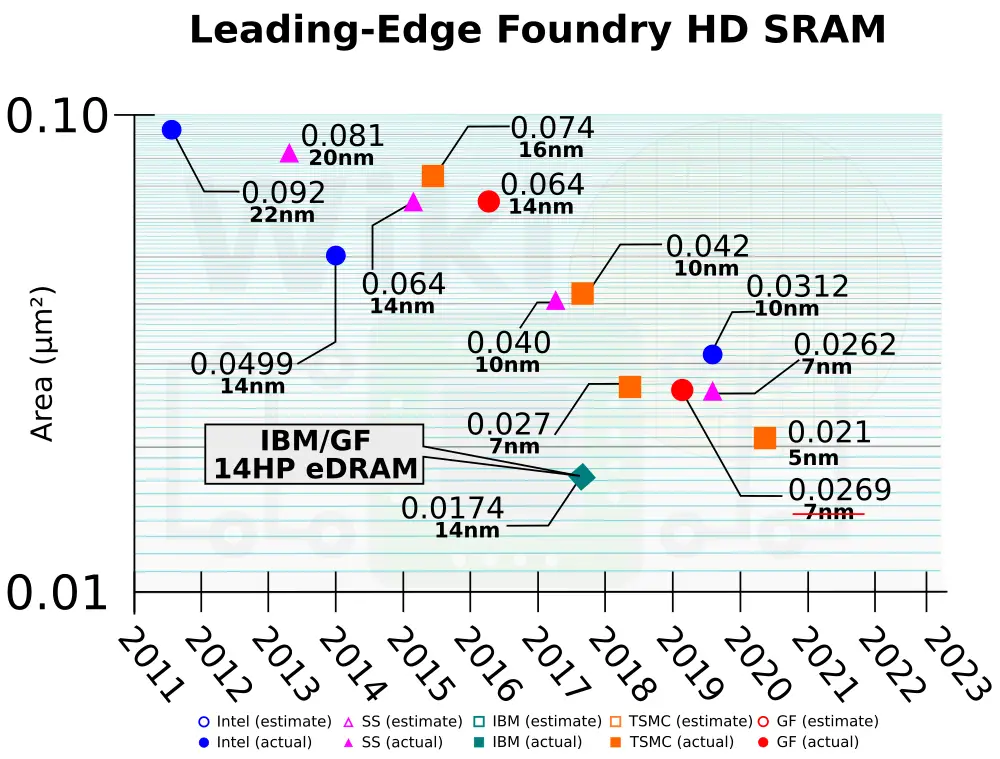
The density what they got on Glo-Fo 14nm (0.0174 μm²) was over 2 time better than SRAM density on TSMC 7nm (0.027 μm²) so a hypothetical eDRAM L3 would probably take less than 50 mm² of die area:

sram-wt-14hp-edram.png


I'm no hardware engineer though so I'm not sure if it would make any sense on a GPU, let alone a consumer-only GPU
 
  • Like
Reactions: Tlh97 and Elfear

Gideon

Golden Member
Nov 27, 2007
1,646
3,712
136
No, it doesnt. Microsoft scraped the idea with the Xbox One X.
Another good point. According to anandtech:

Xbox 360 had 10MB of eDRAM with 32GB/s bandwidth
Xbox One had 32MB of eSRAM with 102GB/s bandwidth

The bandwidth figures are really anemic, I wonder what number IBM got out of their chips? 100 GB/s is less than you get out of 8-channel DDR4. It would have to be nearer to 1TB/s to make any kind of sense.
 

maddie

Diamond Member
Jul 18, 2010
4,747
4,691
136
No, it doesnt. Microsoft scraped the idea with the Xbox One X.
Not saying the 128GB cache is true, but don't mistake one implementation of an idea with the idea itself having no value. In engineering, details are often the difference between failure and success.
 

CastleBravo

Member
Dec 6, 2019
119
271
96
Another good point. According to anandtech:

Xbox 360 had 10MB of eDRAM with 32GB/s bandwidth
Xbox One had 32MB of eSRAM with 102GB/s bandwidth

The bandwidth figures are really anemic, I wonder what number IBM got out of their chips? 100 GB/s is less than you get out of 8-channel DDR4. It would have to be nearer to 1TB/s to make any kind of sense.

Is eDRAM always going to have anemic bandwidth, even on 7nm, and with 128MB vs 10-32MB, or did the MS engineers design those products to meet a certain performance target and not bother going any higher?
 
  • Like
Reactions: Gideon

Olikan

Platinum Member
Sep 23, 2011
2,023
275
126
Dylan522p, from r/hardware...

"As total SRAM, that makes sense actually.

Microsoft claims XSX has a total 76MB SRAM for their 8C, 2SE, 56CU chip.

If we assume that 12MB comes from having extra WGP and the CPU, then we get to 64MB for 2SE and 5 WGP per SA.

Navi 21 is supposed to be 4 SE, so *2 and tada, there's 128MB SRAM."
 

sontin

Diamond Member
Sep 12, 2011
3,273
149
106
Not saying the 128GB cache is true, but don't mistake one implementation of an idea with the idea itself having no value. In engineering, details are often the difference between failure and success.

Microsoft went from 68gb/s to 320gb/s off-chip. I think that is a statement that their approach with the One/S has failed. On-Chip ram must still be refreshed to hold the information and increasing the L2 cache will result in yields problems.
 
  • Like
Reactions: raghu78

Gideon

Golden Member
Nov 27, 2007
1,646
3,712
136
Is eDRAM always going to have anemic bandwidth, even on 7nm, and with 128MB vs 10-32MB, or did the MS engineers design those products to meet a certain performance target and not bother going any higher?
Quick googling lead me to this interesting article from 2014
Intel claims 102.4GB/s at 1W using their OPIO. IBM claims 3TB/s L3 bandwidth (across 12-cores @ 4GHz) with its on-chip eDRAM implementation. Intel’s implementation has provided clear power and performance benefits for its parts, but the IBM results show that there is still more to be had if that eDRAM is placed on chip.
So it should definitely be possible to get > 1TB/s bandwidth from eDRAM @ 2 Ghz, interesting!

I would still like to hear from some hardware guys whether such a large eDRAM cache would make any sense on a consumer GPU.
 

maddie

Diamond Member
Jul 18, 2010
4,747
4,691
136
Microsoft went from 68gb/s to 320gb/s off-chip. I think that is a statement that their approach with the One/S has failed. On-Chip ram must still be refreshed to hold the information and increasing the L2 cache will result in yields problems.
I didn't see L2 cache, just cache. Also cache is easy to make defect resilient, being a simple repetitive structure.
 

jpiniero

Lifer
Oct 1, 2010
14,629
5,245
136
So many comments are about AMD launching later than NVIDIA, so it means rdna2 is not as good as first though. On the contrary, if rdna2 was not good they would launch it on the back of Zen3, so positive news on zen3 would over shadow rdna2.

I think they want to see Ampere reviews and actual availability/prices before committing to saying anything.
 

Saylick

Diamond Member
Sep 10, 2012
3,172
6,408
136
Dylan522p, from r/hardware...

"As total SRAM, that makes sense actually.

Microsoft claims XSX has a total 76MB SRAM for their 8C, 2SE, 56CU chip.

If we assume that 12MB comes from having extra WGP and the CPU, then we get to 64MB for 2SE and 5 WGP per SA.

Navi 21 is supposed to be 4 SE, so *2 and tada, there's 128MB SRAM."
And Andrei from AT said in response, "It infers to a 128MB cache chiplet connected to the GPU. This chiplet would probably also see use in Zen3 CPUs."

I'm not sure how to reconcile this still...
 

Kuiva maa

Member
May 1, 2014
181
232
116
Dylan522p, from r/hardware...

"As total SRAM, that makes sense actually.

Microsoft claims XSX has a total 76MB SRAM for their 8C, 2SE, 56CU chip.

If we assume that 12MB comes from having extra WGP and the CPU, then we get to 64MB for 2SE and 5 WGP per SA.

Navi 21 is supposed to be 4 SE, so *2 and tada, there's 128MB SRAM."

Typically I find that these "out of left field" rumors tend to carry weight. It reminds me of the recent peculiar rumor about the nvidia 12-pin connector or the "crazy bus" when Fiji first appeared in leaked benchmarks before we knew it used HBM. People that try to spread false rumors usually present something expected, to make the rumor plausible.
 

Olikan

Platinum Member
Sep 23, 2011
2,023
275
126
And Andrei from AT said in response, "It infers to a 128MB cache chiplet connected to the GPU. This chiplet would probably also see use in Zen3 CPUs."

I'm not sure how to reconcile this still...
I mean, the pieces of the puzzle kinda makes sense...
1- N21 have 16 slices of L2, this means 256 or 512 memory width... 512 seems very unlike, also we have that photo leak with256-bit

2- a small density increase, and this huge cache can fit with 80Cu... also, Ray Tracing loves huge caches

3- N21 support xGMI, we were all puzzled why...
 

Kenmitch

Diamond Member
Oct 10, 1999
8,505
2,249
136
And Andrei from AT said in response, "It infers to a 128MB cache chiplet connected to the GPU. This chiplet would probably also see use in Zen3 CPUs."

I'm not sure how to reconcile this still...

Hmm.

Hypothetical question....If both have the 128MB could these be part of the hybrid RT solution? Maybe a higher speed interconnect?

Would any of the following patents be applicable?

 
Last edited:

itsmydamnation

Platinum Member
Feb 6, 2011
2,776
3,164
136
No, it doesnt. Microsoft scraped the idea with the Xbox One X.
it wasnt a cache, it was a scratch pad

Microsoft went from 68gb/s to 320gb/s off-chip. I think that is a statement that their approach with the One/S has failed. On-Chip ram must still be refreshed to hold the information and increasing the L2 cache will result in yields problems.

How does increasing sram or edram increase yield problems, they are like the easiest thing to make redundant .
 

senseamp

Lifer
Feb 5, 2006
35,787
6,195
126
Come on, AMD is not shipping a high end GPU with a 256bit bus GDDR6. They got burned time and again with memory weirdness, if they haven't learned their lesson by now, there's really no hope for them. It's probably Navi 22 or a Navi 21 cut down to 256bits that they are using as a placeholder for Navi 22 for their own internal reasons like deferring tape-out costs.
 
  • Like
Reactions: TESKATLIPOKA

Shmee

Memory & Storage, Graphics Cards Mod Elite Member
Super Moderator
Sep 13, 2008
7,409
2,443
146
I would like a 512bit bus, like with Hawaii. At least for the top end, if not using HBM2E.
 

A///

Diamond Member
Feb 24, 2017
4,352
3,154
136
Blame their arrogance towards AMD.

Doesn't quite explain the last few times Nvidia lost to AMD. Granted, few and far in between... Intel didn't think AMD was worthy leading up until March 2017. I know Intel readied themselves for Bulldozer, but when it became apparent that it was a lost cause for AMD, they breathed a sigh of relief.