Radeon Vega Architecture Preview Thread

Page 3 - Seeking answers? Join the AnandTech community: where nearly half-a-million members share solutions and discuss the latest tech.

PhonakV30

Senior member
Oct 26, 2009
987
378
136
:cool:

Geometry throughput slide : Data base on AMD engineering design of Vega.Radeon R9 Fury X has 4 geometry engines and a peak of 4 polygons per clock.Vega is designed to handle up to 11 polygons per clock with 4 geometry engines.This represents an increase of 2.6x
 
Last edited:

Krteq

Senior member
May 22, 2015
991
671
136
Wow, nice geometry throughput increase... so no more geometry bottleneck on AMD cards?
 

Krteq

Senior member
May 22, 2015
991
671
136
Polaris still have 4 geometry engines and a peak of 4 polygons per clock, but zero-area triangles can be discarded during a process thanks to "Primitive Discard Accelerator".
 

Ancalagon44

Diamond Member
Feb 17, 2010
3,274
202
106
What time is the presentation due to start?

ve.ga is not loading for me - timing out.

Will your budget at least stretch for an 8gb 480? If you can find a deal, return the 4gb card for an 8gb 480!

Vega--at least this initial release--is a higher-end line that is not replacing P 10, and will probably be 3+ months away, anyway.

It isn't that I can't afford the 8GB version, it's that I didn't think it was worth the extra money for me, right now.

Having looked at benchmarks of the difference between the 4GB version and the 8GB version, it looks like there is about a 1% difference. So, yes, it might be faster down the line when games use more VRAM, but for now, I'd see 0 difference (zero perceptible difference). Plus, I'm not as heavy a gamer as some people here, so I wasn't sure whether it was worth it for me.

By the time 4GB is too little VRAM, my 480 will be quite weak anyway. So, I'd sell it and buy a 580 or 680 or whatever. But for now, I just didn't see the value in spending the extra amount of money.
 

krumme

Diamond Member
Oct 9, 2009
5,952
1,585
136
Noticed its not 2x throuput per clock like the cloud image but the slide says"over" 2x. Wrooom :)
Edit: behrouz beat me to it i can see. Example in endnotes is 2.6.
 

ShintaiDK

Lifer
Apr 22, 2012
20,378
145
106
Vega chip.
003.jpg
 
  • Like
Reactions: AtenRa

4K_shmoorK

Senior member
Jul 1, 2015
464
43
91
An architecture preview
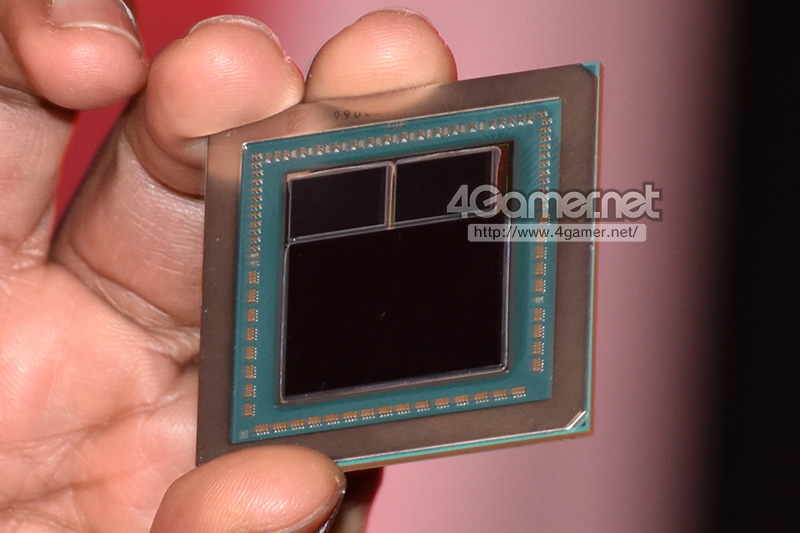
This is an architecture preview hence we do have a thing or two to share with you today. Let's get the elephant out of the room first and confirm something. Yes, VEGA, (well VEGA10) will be fitted with HBM2 memory as well as a new IO gateway and that cache dubbed High Bandwidth Cache. Vega is a GPU with 200 new features. A handful of things are key for AMD with this very scalable GPU new architecture. Now I deliberately state new architecture here as that much is a fact, VEGA is not based upon Polaris, this is a completely new chip and architecture with a new programmable geometry pipeline as well.


index.php


Vega 10 is using High Bandwidth Video Memory, VRAM, graphics memory or whatever you like to call it. The specific type flavor or flavah-flaf used is HBM2 memory. The graphics gawds from AMD claim that HBM2 will offer you 5x the power efficiency compared to any other graphics memory including GDDR5, and yes that is huge. Another benefit obviously is capacity. HBM is on-chip vertically stacked (slabs of memory cells placed on top of each other) and you know it, when it comes to caches and memory bigger is simply better (in terms of storage volume). With the second iteration of HBM, HBM2 AMD now has 8x the density per stack with a 50% smaller footprint. So again, not to confuse anybody, frame-buffer or graphics memory is now referred to as HB (high bandwidth) cache here. I'll let you in on a little secret (AMD has not disclosed this much), but you may can expect 8 GB for the initial VEGA based products.

http://www.guru3d.com/articles-pages/editorial-amd-vega-gpu-architecture-preview,1.html

No details on release date or clock frequencies.
 

MrTeal

Diamond Member
Dec 7, 2003
3,569
1,699
136
Has anyone used vanishing point to estimate the GPU die size from the stacks of HBM2 yet?
 

zinfamous

No Lifer
Jul 12, 2006
110,592
29,221
146
There is already a Vega architecture thread--this article does not need its own thread. Should it not be posted in that thread?
 

Det0x

Golden Member
Sep 11, 2014
1,031
2,962
136
Read somewhere in my early morning sleepiness that its around Hawaii size.

Two estimates so far:

WFJUL3U4.jpeg


http://videocardz.com/65477/amd-vega-gpu-pictured-features-two-hbm2-stacks

Close ups of the GPU posted by TechReport, Computerbase and 4Gamer reveal that the GPU is the biggest FinFET design by AMD. Videocardz also made a comparison that showcases the huge chip against other GPUs such as the NVIDIA GP102, GP102 and AMD’s Fiji GPU. The chip is somewhere in between 530-560mm2 so this is really a monstrous chip design and should pack a lot of power.

http://wccftech.com/amd-vega-gpu-pictures-hbm2-official/
 
Last edited:

thilanliyan

Lifer
Jun 21, 2005
11,871
2,076
126
Hope it mines well :D
I'm in for 2 if it does!! Games still play well enough on my 290s...no reason to upgrade except for better mining efficiency.
 
Last edited:

sm625

Diamond Member
May 6, 2011
8,172
137
106
Those chip resistor packages look like 1.4mm with a 2.0 mm pitch between packages. That puts my estimate at about 25x19. But the spacing is not even so its really not much more than a guess. I cant see it being much over 500 though. How do we know those dies are 11.87mm?