NVIDIA Volta Rumor Thread

Page 10 - Seeking answers? Join the AnandTech community: where nearly half-a-million members share solutions and discuss the latest tech.

raghu78

Diamond Member
Aug 23, 2012
4,093
1,475
136
I assumed that increase in bus width is what is required to properly fed GV architecture, and each generation Nvidia increases the amounts of VRAM available in specific price tiers, and also increased the memory bus width.

For example if they decide to use GV107 with 192 Bit GDDR5X, they can for example offer something like this:
GTX 2050 Ti - 6 GB GDDR5X
GTX 2050 - 3 GB GDDR5. In both cases it would be improvement over the GPUs they replaced. GDDR5X memory controller is backwards compatible with GDDR5.

Nvidia has not increased bus width from the Kepler generation at each product tier. In fact they have reduced bus width with GM106 (128 bit) compared to GK106 (192 bit). Nvidia have been able to feed their GPUs by increasing memory speeds GDDR5 (from 6 Gbps -> 7 Gbps -> 8 Gbps) / GDDR5X (1/11 Gbps) and with improved color compression. Thats why I am quite sure Nvidia will stick to the same memory bus width.
 

Samwell

Senior member
May 10, 2015
225
47
101
I am quite sure that Volta architecture will power the next gen Geforce stack. I think this is how it could turn out

GV102 - 384 bit GDDR6 at 14-16 Gbps - 672 - 768 GB/s
GV104 - 256 bit GDDR6 at 14-16 Gbps - 448 - 512 GB/s
GV106 - 192 bit GDDR5X at 11 Gbps - 264 GB/s
GV107 - 128 bit GDDR5X at 11 Gbps - 176 GB/s

Nvidia would want to keep the memory bus at the same sizes as Pascal as that would allow them to keep memory I/O power and board costs under control. Thats the reason I do not see Nvidia increase memory bus width for GV106/GV107. Volta is shaping up to be a true powerhouse and could go down as one of the most successful and forward looking GPU architectures ever after the legendary G80.

Yes, i expect the same. Maybe 12Gbps Ram for Full GV106/GV107. But the shaders are also pretty easy to guess for GV102-GV106. Just GV107 is not so clear. I bet it looks like this:

GP102 30x128SP 3840 -> GV102 42x128SP = 5376SP =6GPCs
GP104 20x128SP 2560 -> GV104 28x128SP = 3584SP =4GPCs
GP106 10x128SP 1280 -> GV106 14x128SP = 1792SP =2GPCs
GP107 6x128SP 768 -> GV107 7-8x128SP = 896-1024SP =1GPC

GV100 has also 6GPCs with 7SMM per GPC. That's up from 5 SMM/GPC in most Pascal, which safes diespace. GP107 was an anomally, it seem they thought 1 standard GPC would be to slow and put 6 smm inside, so maybe GV107 could be also 8smm with 1024SP. But keeping 7SMM/GPC minimizes design efforts and they should have a pretty nice lineup.
 
Last edited:

IntelUser2000

Elite Member
Oct 14, 2003
8,686
3,785
136
Yeah. I don't think anyone should expect that. That is how you end up with Vega level disappointment. People read about new Vega features and start assuming IPC increases of 30%, and then it gets delivered and no IPC gains materialize...

I agree. I'm expecting 20-30% for Volta. Same as they achieved with Pascal. 50% might happen but maybe a year later with higher product stack like they do with ti products.

A significant die size increase is more justified for GV100 because its selling for super high prices and manufacturing prices are absolutely dwarfed. In the consumer sector they'll have to be more careful with costs.
 
  • Like
Reactions: Kuosimodo

Glo.

Diamond Member
Apr 25, 2015
5,642
4,382
136
I agree. I'm expecting 20-30% for Volta. Same as they achieved with Pascal. 50% might happen but maybe a year later with higher product stack like they do with ti products.

A significant die size increase is more justified for GV100 because its selling for super high prices and manufacturing prices are absolutely dwarfed. In the consumer sector they'll have to be more careful with costs.
Which Pascal? GP100 or consumer chips?

Because consumer Pascal delivered zero IPC increase over Maxwell because it used the same architecture layout. If Nvidia will shift from 128 cores/256 KB Register file size to 64 core/256 RFS we will see increase in IPC, just like we have seen with Maxwell vs Kepler.
 

Qwertilot

Golden Member
Nov 28, 2013
1,604
257
126
I agree. I'm expecting 20-30% for Volta. Same as they achieved with Pascal. 50% might happen but maybe a year later with higher product stack like they do with ti products.

A significant die size increase is more justified for GV100 because its selling for super high prices and manufacturing prices are absolutely dwarfed. In the consumer sector they'll have to be more careful with costs.

It'll be almost exactly what they achieved with Pascal - that's what they've clearly calculated as being enough to drive annual upgrades :) Hence they'll tweak die sizes etc to make it - the need to get those annual upgrades & associated massive revenues will though I think basically over rule any thoughts regarding manufacturing costs.
 

Konan

Senior member
Jul 28, 2017
360
291
106
What are the odds of a Pascal refresh prior to a Volta consumer release? I know there was talk earlier in the year, but is that a dead thought process?
 

jpiniero

Lifer
Oct 1, 2010
14,487
5,155
136
What are the odds of a Pascal refresh prior to a Volta consumer release? I know there was talk earlier in the year, but is that a dead thought process?

The mining craze and Vega's relative underperformance may have killed off any desire to do it.
 
  • Like
Reactions: Kuosimodo

Rifter

Lifer
Oct 9, 1999
11,522
751
126
The mining craze and Vega's relative underperformance may have killed off any desire to do it.

I agree, if anything Nvidia will now use this time to build up some good stock and get driver software all smoothed out for a smooth volta launch.
 

Cookie Monster

Diamond Member
May 7, 2005
5,161
32
86
Yes, i expect the same. Maybe 12Gbps Ram for Full GV106/GV107. But the shaders are also pretty easy to guess for GV102-GV106. Just GV107 is not so clear. I bet it looks like this:

GP102 30x128SP 3840 -> GV102 42x128SP = 5376SP =6GPCs
GP104 20x128SP 2560 -> GV104 28x128SP = 3584SP =4GPCs
GP106 10x128SP 1280 -> GV106 14x128SP = 1792SP =2GPCs
GP107 6x128SP 768 -> GV107 7-8x128SP = 896-1024SP =1GPC

GV100 has also 6GPCs with 7SMM per GPC. That's up from 5 SMM/GPC in most Pascal, which safes diespace. GP107 was an anomally, it seem they thought 1 standard GPC would be to slow and put 6 smm inside, so maybe GV107 could be also 8smm with 1024SP. But keeping 7SMM/GPC minimizes design efforts and they should have a pretty nice lineup.

I remember doing something similar to speculate on potential consumer Volta parts:

...if we look at the downscaling of GP100 to the consumer orientated GP102, we could expect a hypothetical ~627mm2 GV102 with 5376CC (64CC per SM/14SM per GPC/6GPC) with a 384bit GDDR5X/6 memory system. This is probably sometime next year.

Using the same method (GP102 -> GP104), GV104 which could get released this year is in the vincinity of ~418mm2 with 3584CC (64CC per SM/14SM per GPC/4GPC) and 256bit GDDR5/5X/6 memory system. All this assumes that the volta based geforce variants shares some similarities to its compute version (like how SMs are partitioned etc). If its Pascal on steroids, then it may also be different. Thinking its more of the former and would be interesting to know how they achieved a 50% in efficiency in their SMs with Volta over Pascal (This would be hugely beneficial given they are stuck on 16nm or 12nm)

Whether or not it will be 64CC per SM for a total of 14SM per GPC vs 128CC per SM for a total of 7SM per GPC, I think its fare enough to expect a GV104 to perform at around GP102 levels (+10~20%; higher would be a bonus) all at a lower power consumption thanks to GDDR6, possibly a better process node (12nm?) and architectural improvements.

I can't see how AMD will be able to compete with Volta tbh when the Volta x70 and x80 cards will be at 1080Ti level of performance..
 

IntelUser2000

Elite Member
Oct 14, 2003
8,686
3,785
136
Hence they'll tweak die sizes etc to make it - the need to get those annual upgrades & associated massive revenues will though I think basically over rule any thoughts regarding manufacturing costs.

The significant rework they need to do by taking out the tensor units and much reduced DP is also the reason why its likely they'll have to stagger the launch as they did with previous generations.
 

Ajay

Lifer
Jan 8, 2001
15,332
7,792
136
Yes, i expect the same. Maybe 12Gbps Ram for Full GV106/GV107. But the shaders are also pretty easy to guess for GV102-GV106. Just GV107 is not so clear. I bet it looks like this:

GP102 30x128SP 3840 -> GV102 42x128SP = 5376SP =6GPCs
GP104 20x128SP 2560 -> GV104 28x128SP = 3584SP =4GPCs
GP106 10x128SP 1280 -> GV106 14x128SP = 1792SP =2GPCs
GP107 6x128SP 768 -> GV107 7-8x128SP = 896-1024SP =1GPC

GV100 has also 6GPCs with 7SMM per GPC. That's up from 5 SMM/GPC in most Pascal, which safes diespace. GP107 was an anomally, it seem they thought 1 standard GPC would be to slow and put 6 smm inside, so maybe GV107 could be also 8smm with 1024SP. But keeping 7SMM/GPC minimizes design efforts and they should have a pretty nice lineup.

These die size will be too large, IMHO. Unless you have some evidence supporting these numbers, I am very skeptical. TSMC's 12FFC only offers a small density improvement over it's 16FF+ process. Volta AIBs are supposed to be more expensive than Pascal, but this would likely be due to increased memory costs alone. I could be wrong - we will see.
 
  • Like
Reactions: Pick2

PeterScott

Platinum Member
Jul 7, 2017
2,605
1,540
136
These die size will be too large, IMHO. Unless you have some evidence supporting these numbers, I am very skeptical. TSMC's 12FFC only offers a small density improvement over it's 16FF+ process. Volta AIBs are supposed to be more expensive than Pascal, but this would likely be due to increased memory costs alone. I could be wrong - we will see.

I agree. His example is 40% more SPs which given the minimal density increase in 12nm FFN, will lead to almost 40% larger GPU die size, meaning they would likely increase by a full cost tier to make up for the extra die size. Especially considering the current non competitive market, and mining impact on pricing. So Yay, a GTX 2060 will perform like a GTX 1070, but end up costing just as much...

I expect a more modest increase in SPs (say 20%) and some extra IPC improvement in some cases.
 

Bouowmx

Golden Member
Nov 13, 2016
1,138
550
146
The supporting "evidence" is that the supposed GV10[246] core count are of the same proportion to GV100, as GP10[246] are to GP100.

Code:
| Processor | Cores | Area (mm^2) | Cores/area (mm^-2) |
|-----------|------:|------------:|--------------------|
| GP100     |  3840 |         610 | 6.29508196721311   |
| GP102     |  3840 |         471 | 8.15286624203822   |
| GP104     |  2560 |         314 | 8.15286624203822   |
| GP106     |  1280 |         200 | 6.4                |
| GV100     |  5376 |         815 | 6.59631901840491   |
| GV102     |  5376 |         629 | 8.54300339963269   |
| GV104     |  3584 |         420 | 8.54300339963269   |
| GV106     |  1792 |         267 | 6.70625766871166   |

GV areas are calculated as follows:
(GV cores)/((GP cores/area) * ((GV100 cores/area)/(GP100 cores/area)))

Example with GV102:
(GV102 cores)/((GP102 cores/area) * ((5376/815 mm^2)/(3840/610 mm^2)))
5376/((3840/471 mm^2) * 1.048)
629 mm^2

Note that these estimates are likely over-estimates, because they include area-increasing tensor cores.
 

Glo.

Diamond Member
Apr 25, 2015
5,642
4,382
136
The 12 nm FFN process should be around 20% more dense than 16 nm FF+, that current GP10x GPUs are made on.

Also, you accounted the die sizes, but not accounted for changed layout of the architectures, different memory controller counts, etc. IMO GV104 will not have over 400mm2.

Also I do not believe that for GV104 to be 30% faster than GTX 1080 Ti is required more than 3072 CC's that are using Volta architecture.

20% more Cores, with 50% more IPC, thanks to shift from 128Core/256 Register File Size, to 64 core/256 RFS, gets you around 65-70% increase in performance, at the same clock, as GTX 1080 had.

Only problem you get is that the throughput of the cores is so big that you have to have enough memory bandwith and very fine grained scheduling to feed the cores, all of the time.

I think xpea some time ago has written that Volta will have Tensor cores in some way/ shape or form on consumer GPUs, for compatibility reasons, which may suggest that we will actually see true Volta architecture, instead of reused, repurposed GP100 architecture, which also would have same 64core/256 RFS, but not that good scheduling, as Volta has(which is very important, also since you have such high throughput of the cores...).


Next topic: GDDR5 prices. Currently 20 nm GDDR5 prices went up by 30% to around 6$ price tag per chip. This makes GP107 memory subsystem to cost Nvidia not 18$ like it was before, but 24. That is 6$ increase, and we can expect that this GPU price will go up by 10$, in upcoming months.

However, Micron and SK Hynix are going to manufacture GDDR5 16 nm in 2018. What this means is that prices for this memory will go down by around 50%, to 3$. For GV107, most economically affordable, and logical move will be running 192 Bit memory bus, because GDDR6 memory will cost around 10$, for each chip. 40$ for 256 GB/s memory bandwidth, vs 18$ for 192 GB/s? Its way easier to get to 149$ price tag with 18$ memory subsytem rather than 40$ ;).

Also consider this: GV104 will use GDDR6, on a 256 bit memory bus. That makes it 8 chips, for around 10$, each.

Well, this GPU will not be cheap. I expect the same rollout as for Pascal was: first GV104 - GTX 2080 costing 699$.

Those are just my thoughts on what might happen.
 

nvgpu

Senior member
Sep 12, 2014
629
202
81
GV104 GTX 2080(?) will be $599 just like GP104 GTX 1080 in 2016, Nvidia already seen the bad reactions and feedback from the Founders Edition pricing and they're not gonna repeat that.

192bit is unlikely for GV107, you'll have to use more expensive PCB with more traces for the extra memory chips.

http://www.anandtech.com/show/11398...am-gddr6-added-to-catalogue-gddr5-gets-faster

It's more likely that GV107 will use the slowest 12GT/s GDDR6 memory, 4 memory chips x 48GB/s is 192GB/s of memory bandwidth, just right.
 
Last edited:
  • Like
Reactions: Bouowmx

Dayman1225

Golden Member
Aug 14, 2017
1,152
973
146
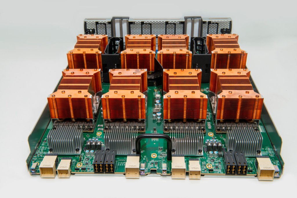
DJIvAu0WAAAjkwM.jpg:large


Nvidia DGX - 1 Volta, god damn is that beautiful or what!
 
  • Like
Reactions: Bouowmx and DooKey

Rifter

Lifer
Oct 9, 1999
11,522
751
126
Have they released a launch date for this yet officially? or are we looking at just sometime early next year.
 

Qwertilot

Golden Member
Nov 28, 2013
1,604
257
126
Have they released a launch date for this yet officially? or are we looking at just sometime early next year.
The latter - they've released the ginormous compute based Volta already but it'll take a little while for everything to make sense at consumer volume & pricing.

Sent from my XT1635-02 using Tapatalk
 

Samwell

Senior member
May 10, 2015
225
47
101
These die size will be too large, IMHO. Unless you have some evidence supporting these numbers, I am very skeptical. TSMC's 12FFC only offers a small density improvement over it's 16FF+ process. Volta AIBs are supposed to be more expensive than Pascal, but this would likely be due to increased memory costs alone. I could be wrong - we will see.

I dont think so. It should be possible to get these numbers into 600mm², 400mm² like with Maxwell. Bouowmx already showes the scaling which are worst case numbers, but a gaming chip will be smaller. GP102 will only scale shaders up and features. V100 had Tensor Cores, 50% more nvlinks, 2mb additional l2 cache and 45% more l1/Shared Memory per SM compared to GP100. And nevertheless they increased shader count by 40% with just 33% more die size.

GV102 won't have tensor cores (maybe a few for compatibility), won't have interfaces like nvlink which need to scale, probably won't have a increased l2 cache and scaling of L1 Cache will probably be between 15-33%. Additionally we have the 12FFN process which is unknown. Just because GV100 doesn't show scaling means nothing. Building such a big chip with a bit lower density might improve yield substantially. GV102 might have a 5% higher transistor density and then you're easy under 600mm².
 

PeterScott

Platinum Member
Jul 7, 2017
2,605
1,540
136
I dont think so. It should be possible to get these numbers into 600mm², 400mm² like with Maxwell. Bouowmx already showes the scaling which are worst case numbers, but a gaming chip will be smaller. GP102 will only scale shaders up and features. V100 had Tensor Cores, 50% more nvlinks, 2mb additional l2 cache and 45% more l1/Shared Memory per SM compared to GP100. And nevertheless they increased shader count by 40% with just 33% more die size.

That had negligible effect. They increased the transistor count by 38%, and the cuda cores by 40%, which means the impact of the other systems on transistor budget was negligible. So it will take about 33% more die size to increase core counts by about 40%.

If you think NVidia is going to increase die size by 33% and not increase price by similar amount(or more), you aren't aware of the competitive landscape, or the state of Moore's law.

We are hitting a process wall, and I expect more conservative jumps in core counts going forward. 20% then 20% giving Nvidia two generations of moderate gains rather than one big one.
 
Last edited:
  • Like
Reactions: Rifter

Rifter

Lifer
Oct 9, 1999
11,522
751
126
That had negligible effect. They increased the transistor count by 38%, and the cuda cores by 40%, which means the impact of the other systems on transistor budget was negligible. So it will take about 33% more die size to increase core counts by about 40%.

If you think NVidia is going to increase die size by 33% and not increase price by similar amount(or more), you aren't aware of the competitive landscape, or the state of Moore's law.

We are hitting a process wall, and I expect more conservative jumps in core counts going forward. 20% then 20% giving Nvidia two generations of moderate gains rather than one big one.

Sadly likely true. AMD is applying no pressure so Nvidia has no reason to shoot for the moon. Vega doesnt compete effectively vs pascal let alone volta. If there was ever a generation when Nvidia could sit back and milk us for all we are worth now is it.
 

Qwertilot

Golden Member
Nov 28, 2013
1,604
257
126
Sadly likely true. AMD is applying no pressure so Nvidia has no reason to shoot for the moon. Vega doesnt compete effectively vs pascal let alone volta. If there was ever a generation when Nvidia could sit back and milk us for all we are worth now is it.
They'll give us the usual jump :) They've been utterly consistent in doing that fur ages now.

There's 7nm coming onstream for son of Volta, so no particular reason to really pull punches quite yet.

What they'll do after two generations on 7nm, well, goodness knows!

Sent from my XT1635-02 using Tapatalk
 
  • Like
Reactions: Head1985

PeterScott

Platinum Member
Jul 7, 2017
2,605
1,540
136
They'll give us the usual jump :) They've been utterly consistent in doing that fur ages now.

There is no "usual" jump.

GTX 660 ( GK 106) 960 cores (sep-2012)
GTX 960 ( GM 206) 1024 cores (Jan-2015) 6.7% increase
GTX 1060 (GP 106) 1280 cores (Jul-2016) 25% increase

Not sure how you look at this and think a 40% core count increase is the consistent jump?