New Zen microarchitecture details

Page 100 - Seeking answers? Join the AnandTech community: where nearly half-a-million members share solutions and discuss the latest tech.

looncraz

Senior member
Sep 12, 2011
722
1,651
136
Now you are shifting the goalposts, or maybe AMD itself was being duplicitous in making the calculation.

No, I showed another way this time around, my first example was the entire board power. Originally, AMD only mentioned 2.8x performance in relation to Polaris. Only later did this get stuck on the RX 480 product in a few slides - which could be a communication issue, or it could be due to the use of a method similar to mine, or it could be because they compared using TDP rather than actual consumption.

My only real interest is in what the process achieved for Polaris 10 - and 2.8x is within the region of what is observed (lower power, higher clocks). I don't think AMD was being deceitful, I think RX 480 power consumption is 15W too high - which may be entirely due to the VRM usage not being included in their board logic (the VRM uses about 16W under full load, AFAICT).

As others have mentioned, it is expected for the RX 470 to use less power yet not give up much performance. Some rumors are as high as 95% of the 4GB card's performance, but only 90% of the power draw.

But as the majority of people assume the meaning to be, 2.8x performance per watt increase means 2.8 faster FPS for the same power usage by the entire card.

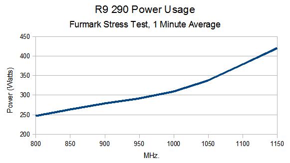
According to Anandtech, the stock R9 290 uses 88W more in Crysis 3 (so 165W vs 253W), but the RX 480 performs 3.8% better. That is only 1.6x improvement by that method - which is no less valid of a method, no doubt, but it measures a different type of efficiency (FPS/W, rather than W/CU/HZ - which is the concern for process-derived improvements).

But, that little "up to" gives so much room to wiggle that we have to look at other FPS/W or Perf/W scenarios... because only one is needed to be true by this method. The closest I've found is TessMark, at 2.35x.

However, if we use each card's TDP, things get interesting. Crysis 3 shows a 1.9x improvement, and Tessmark shows a 2.81x improvement.

Really can't help but to wonder if this is what someone did at AMD. Kind of makes sense... some management type said: 150W TDP, 275W TDP, Tessmark result is 53% faster, that gives... 2.81x performance/w improvement. Sweet, run with it!

OR, they could compare it with the R9 380... and use TDP comparisons... numbers don't change much for most games, interestingly, though the best result is in Lux Mark at 2.44x, and Tessmark becomes just 1.82x.

In fact introducing other variables such as clockspeed, process, and ram power usage, you are doing exactly what you said is not part of the "scientific method": examining several variables at once.

No, I'm removing variables by fixing values in place and comparing like to like.

The FPS/W metric does not do this except at the macro level (comparing one product directly with another). It is immensely useful for the end consumer, no doubt, but much less so for someone interested in the technical improvements of the process (which is my focus).

I'm not saying AMD should have rolled around saying 2.8x performance/watt improvement. I firmly believe under-hyping products is something AMD needs to learn has value. nVidia said almost nothing about the GTX 1060 until it was about to be released. And it will sell like hotcakes nonetheless. I am just saying that the accuracy of the 2.8x claim completely depends on the little footnote AMD has for their claims.

Now if the 470 meets that target, or if they were using some other way to calculate "performance per watt" they technically may have met the criteria, but in a what I consider a deceptive manner.

If AMD believed they had met their goal from internal testing and only realized they failed it after the next few thousand GPUs were sent into the wild and tested by dozens of people, then they weren't being deceptive, they simply missed the target they thought they had achieved.

I even think the 2.8x figure was first leaked before AMD had a prototype die, but I don't have time to check on that, ATM.

EDIT:

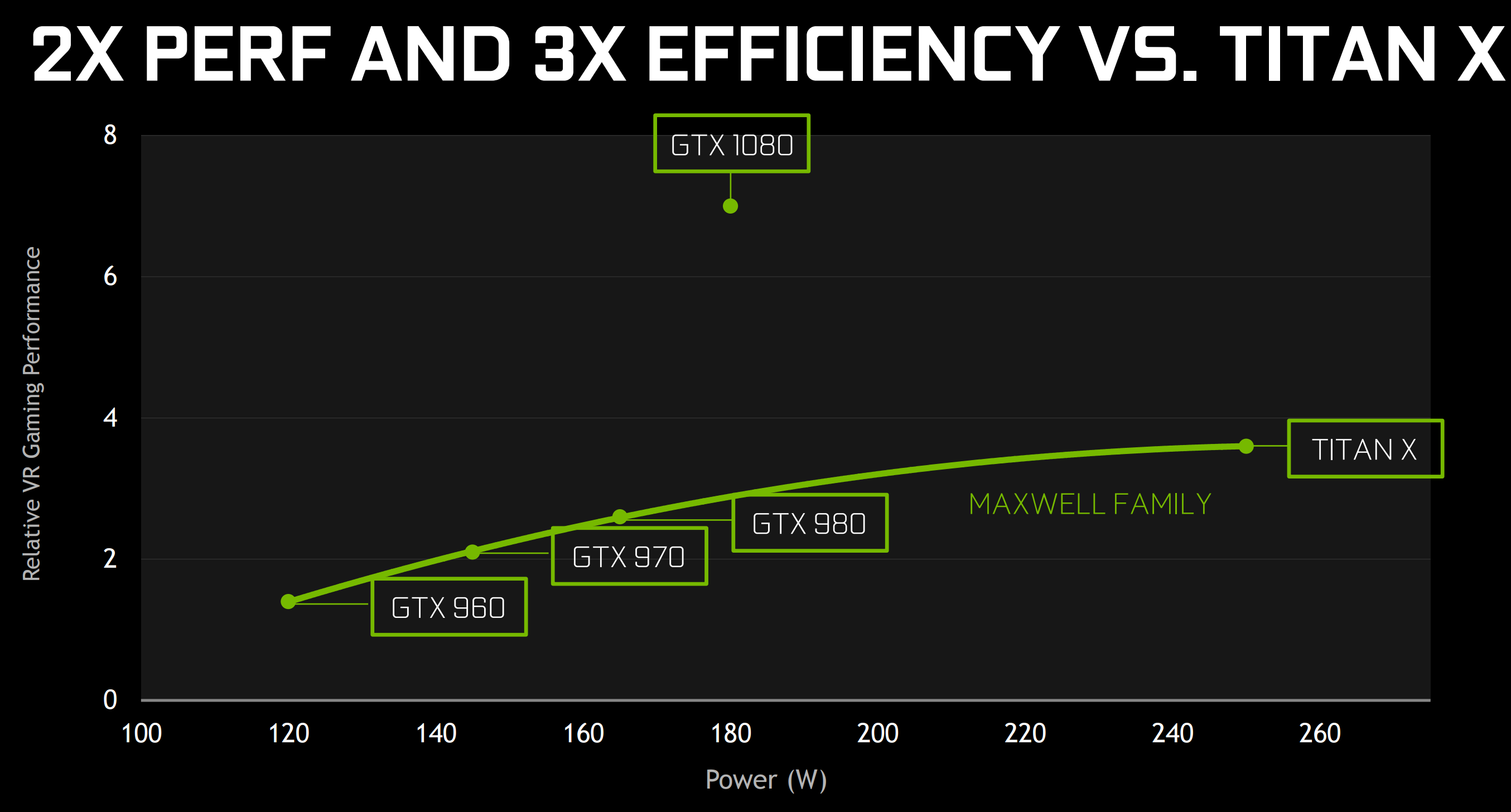
And it's not like nVidia doesn't do the same... or worse:

Nvidia-Pascal-GTX1080-v-Maxwell-performance.png
 
Last edited:

looncraz

Senior member
Sep 12, 2011
722
1,651
136
You like the idea of "equalizing" clocks past the 28nm max stock clocks? Can't wait to see how much PPW Pascal has over a 2Ghz Maxwell.

I did it for 1.84Ghz and got exactly 2.0x.

Mind you, I'm also plotting conservative power curves based on lower differences in clocks (with three points), so I'm not including run-away power consumption figures that can sometimes occur, just what each architecture and process does within its normal operating window and slightly above it.

I have many years of experience doing interpolation and projections of this type and tend to be accurate enough :whiste:

However, I would prefer to have 1Ghz numbers for each card. I much prefer keeping everything even physically measured rather than creating expected values from which to base further estimations.

At 1Ghz, my R9 290 uses much less power than at 1.15Ghz, that's for sure - at just 310W. It jumps to 340W at 1050Mhz, 380W at 1100Mhz, and 420 at 1150Mhz. You might notice that curve isn't terribly steep, even though each jump is a large increase in consumption.

BTW, my R9 290 figures are all one minute averages in Furmark stress test. At 1100Mhz my R9 290 can consume 400W by the end of the test, when it is running at 90C (at 1150C, after just over one minute, I hit 95C, so I don't go any further than that - and I don't like to run it at that), but it uses less when it is cooler - so heat related leakage is certainly a factor (and is part of the increase in rise, I believe, after 1Ghz):

R9_290_Power.jpg


Power limit is always maxed, as well, which will undoubtedly have some serious impact on my numbers for Furmark as my numbers are with no throttling occurring.

I used fewer datapoints for GTX 1060, and I didn't save the spreadsheet for some reason, so I don't have a chart :oops:.
 

Enigmoid

Platinum Member
Sep 27, 2012
2,907
31
91
You have to compare apples to apples.
.....

Proceeds to compare to overclocked 290X.

LOL

Apple to Apples is each GPU operating at their maximally optimum point, or the maximally desired point (which is iffy).

Then, acknowledging each GPU is different and strict comparisons are ultimately impossible (Compare the 1060 vs. the 480 using your methodology - You can't because Pascal and GCN4 are completely different and the same normalization attempts you are making simply do not apply) you simply take the most foolproof and real world example - take performance and divide by power.

This is the most foolproof method. Any other method introduces more error. This is incidentally the method the vast majority of this forum used prior the the 480s launch.

Remember that 2.8x takes these factors into account. There is no need to specifically try to decipher them.

The other side is that AMD really did get 2.8x for their calculations. In that case, seeing how the 480 lines up in the real world AMD is doing shady (dishonest) calculations, specifically towards how they are presenting the numbers.
 

Enigmoid

Platinum Member
Sep 27, 2012
2,907
31
91
Of course Nvidia did the same. It seems everyone is at the very least strongly exaggerating how well their products are performing.

AMD used 2.8x performance/W. Not some W/CU/Hz.

I did it for 1.84Ghz and got exactly 2.0x.

Mind you, I'm also plotting conservative power curves based on lower differences in clocks (with three points), so I'm not including run-away power consumption figures that can sometimes occur, just what each architecture and process does within its normal operating window and slightly above it.

I have many years of experience doing interpolation and projections of this type and tend to be accurate enough :whiste:

However, I would prefer to have 1Ghz numbers for each card. I much prefer keeping everything even physically measured rather than creating expected values from which to base further estimations.

At 1Ghz, my R9 290 uses much less power than at 1.15Ghz, that's for sure - at just 310W. It jumps to 340W at 1050Mhz, 380W at 1100Mhz, and 420 at 1150Mhz. You might notice that curve isn't terribly steep, even though each jump is a large increase in consumption.

BTW, my R9 290 figures are all one minute averages in Furmark stress test. At 1100Mhz my R9 290 can consume 400W by the end of the test, when it is running at 90C (at 1150C, after just over one minute, I hit 95C, so I don't go any further than that - and I don't like to run it at that), but it uses less when it is cooler - so heat related leakage is certainly a factor (and is part of the increase in rise, I believe, after 1Ghz):

R9_290_Power.jpg


Power limit is always maxed, as well, which will undoubtedly have some serious impact on my numbers for Furmark as my numbers are with no throttling occurring.

I used fewer datapoints for GTX 1060, and I didn't save the spreadsheet for some reason, so I don't have a chart :oops:.

Please tell me you seriously have not been using a power virus for your power numbers.
 

dark zero

Platinum Member
Jun 2, 2015
2,655
138
106
I wish AMD just licensed IBM's cache system from the power8 and placed it on Zen. Looks like the Power8 does a really good job from the anandtech article.
I feel that is not a wish... seems that AMD is about to get that thanks to GloFo.... yeah... that deal between GloFo and IBM won't come alone...
 

looncraz

Senior member
Sep 12, 2011
722
1,651
136
Of course Nvidia did the same. It seems everyone is at the very least strongly exaggerating how well their products are performing.

AMD used 2.8x performance/W. Not some W/CU/Hz.

Performance/W, for a GPU engineer, IS W/CU/Hz (or some variation thereof).

Watts per compute unit per hertz.

It is a performance-metric agnostic measurement that is most often used to establish the effectiveness of a single change. Since our two modified variables are CU count and frequency, we measure in term of W/CU/Hz. Anything else would be improper.

Please tell me you seriously have not been using a power virus for your power numbers.

Of course I did. I am looking for the worst-case power draw from the cards as they are maximally stressed. I can't get reliable numbers otherwise. The relative deviation for both sets of numbers for gaming vs stressed are rather similar anyway, so it's a moot point.
 

superstition

Platinum Member
Feb 2, 2008
2,219
221
101
Apple to Apples is each GPU operating at their maximally optimum point
What if the maximum performance-per-watt is a clock much lower than what pretty much everyone runs the part at? That would make the comparison more academic than practical.

I've read comments in a number of places where people basically say they don't run the GTX 980 at stock. They always overclock it. Well, the GTX 980's particularly good performance-per-watt in DX11 (and, importantly to me — performance per decibel) figures rest on the conservative stock clockspeed, right?

It seems that there are always arbitrary decisions to be made. I don't think comparing two processes at the same clock is a bad thing at all. It can really highlight the improvement from node shrinkage in particular.

One of the big knocks against 32nm AMD FX has been that, despite significant performance improvements from overclocking that can be found with a chip like the inexpensive 8320E, the power consumption required makes it a dubious choice for some workloads. That speaks directly to the issue of clockspeed — with the part having quite a wide range of operational clocks as well as user-chosen and factory-chosen operational clocks. It also throws performance-per-watt into question as being super-important, too — but that's a different issue.

There are so many variables (library type, VRAM bus width, "pure" gaming design versus workstation functions included — e.g. GF100, die size, thermal transfer/cooling efficiency, architectural balance/efficiency, etc.).

It is true that the "same clock" test can't present the definitive picture. Comparing two parts from two processes at their ideal clocks also is questionable, if the performance of one is quite a lot behind what is considered acceptable (particularly if that part is nearly always overclocked to utilize its additional headroom) and/or the part wasn't sold on the market at that near that clock. Should we look at the stock 8320E or 8370E exclusively when speaking of the general performance-per-watt of FX 8 integer core processors and the 32nm SOI process? Should we look at the 9350?

It seems that doing both types of comparison (equal clock/equal clock and ideal clock/ ideal clock) and looking at the result is the best course of action. In fact, I would take the stock clock from both parts to make two clockspeed tests — one at the one clock, the other at the other clock. Then, a third test with the ideal performance-per-watt clock would be the third test.

(Maybe my thinking is muddled because it's so late but at least I'm trying to be helpful.)

Of course I did. I am looking for the worst-case power draw from the cards as they are maximally stressed. I can't get reliable numbers otherwise. The relative deviation for both sets of numbers for gaming vs stressed are rather similar anyway, so it's a moot point.
Haven't Nvidia and AMD been intentionally throttling things like Furmark in hardware with some designs?
 

looncraz

Senior member
Sep 12, 2011
722
1,651
136
Proceeds to compare to overclocked 290X.

LOL

Apple to Apples is each GPU operating at their maximally optimum point, or the maximally desired point (which is iffy).

As I have repeatedly said if I had 1Ghz value for RX 480 I'd prefer to use those, for that exact reason... however, as my numbers show, there isn't a step change in the R9 290 power curve. I could flatten and rerun the numbers if I had enough RX 480 numbers to do the same - but I don't.

But we'll do it anyway...

Linear interpolation from the 800 to 1Ghz range would then suggest R9 290 should pull 370W at 1.15Ghz, versus the 420W observed.

This means that cutting 4 CUs would save less power than it would have before, but the memory savings are still present. The reconfigured R9 290 (36CUs, 8-channel GDDR5 8Gbps RAM) pulls 335W, compared to the RX480's 165W.

That gives 'just' a 2.03x improvement over Hawaii - or statistically identical to the improvement seen with the GTX 1060.

Then, acknowledging each GPU is different and strict comparisons are ultimately impossible (Compare the 1060 vs. the 480 using your methodology - You can't because Pascal and GCN4 are completely different and the same normalization attempts you are making simply do not apply) you simply take the most foolproof and real world example - take performance and divide by power.

Yes, you can compare disparate architectures this way. You just have to make another psuedo product. This would be a meaningless endeavor, though, as you usually compare end products within families or between similar generations.

This is the most foolproof method. Any other method introduces more error. This is incidentally the method the vast majority of this forum used prior the the 480s launch.

Yes, nothing wrong with using that method at all, except when trying to figure out anything in regards to the process efficiency. I don't know how many times I have to say that I don't care about anything else in regards to this for you to comprehend why I am examining it the way I am.

My interest is in the PROCESS. Not the product. I was countering a negative viewpoint related to 14nm LPP vs 28nm LPP, and my examinations show that 14nm LPP is performing exactly as expected relative to 16FF+, and that it does appear to be marginally superior from a power-efficiency standpoint.

The GPU itself is, in fact, up to 2.8x more efficient given the hardware it includes and its frequency. In certain types of performance, it ALSO is up to 2.8x more efficient... if you use TDP vs TDP... but that's more so the exception than the rule. It tends closer to the 2.0x area, which is still nothing to scoff at.

The other side is that AMD really did get 2.8x for their calculations. In that case, seeing how the 480 lines up in the real world AMD is doing shady (dishonest) calculations, specifically towards how they are presenting the numbers.

They presented these numbers based on projections more like the ones I did here. They don't have the luxury of bench-marking a GPU that doesn't exist, so they have to extrapolate (via simulation) the numbers. Their early dies would have been the most cherry-picked dies, with the expectation that they would have that type of end result. They likely saw 150W (or maybe even lower) power usage considering the variability observed in the wild. They likely did not even have the 1.266Ghz clock speed finalized when those slides were made - if they were thinking ~1Ghz and that the drivers were going to bring about a quick 15% boost, you have a ~130W power draw and similar performance... that's ~2.4x higher efficiency... based on the 275W TDP... which would be similar to a FPS/W measurement.

Did AMD put out 2.8x with their advertising claims? Because I only remember seeing it on technical slides - which are riddled with footnotes.
 

superstition

Platinum Member
Feb 2, 2008
2,219
221
101
My interest is in the PROCESS. Not the product. I was countering a negative viewpoint related to 14nm LPP vs 28nm LPP, and my examinations show that 14nm LPP is performing exactly as expected relative to 16FF+, and that it does appear to be marginally superior from a power-efficiency standpoint.
Apple products using Samsung's 14nm are having worse performance characteristics than TSMC 16nm chips, right?
 

looncraz

Senior member
Sep 12, 2011
722
1,651
136
Haven't Nvidia and AMD been intentionally throttling things like Furmark in hardware with some designs?

I know they used to, but now they seem to just rely on the power limit. If I leave the power limit alone it throttles at 300W no matter what. The 50% power limit allows me to get to 450W before the next throttle point, so I can test up to 1.15Ghz (my card can probably go higher, but not without voltage tweaks).
 

KTE

Senior member
May 26, 2016
478
130
76
BTW did AMD make that 2.8x claim or GF?

Also if AMD, did they preface performance by 'process'?

Sorry, I'd just like to know what the commotion is about, even though I personally think Polaris and linked are outside the scope of this topic. Especially in this much detail.

Sent from HTC 10
(Opinions are own)
 

IntelUser2000

Elite Member
Oct 14, 2003
8,686
3,785
136
XBox One actually only has 68GB/s of memory bandwidth which is then augmented by a small 32MB eSRAM cache. It has zero memory compression with 768 GCN 1.1 SPs running at 853Mhz. That's 'just' 1.23TFLOPS of total shader power.

The consoles may not have brute force power, but the games look absolutely fantastic. That's a natural sacrifice between flexibility you get with PC, and efficiency with dedicated gaming devices like consoles, even if the hardware is identical.

Also, there's diminishing returns with vision too. You get used to 1080p resolutions with no AA or AF. Most games have so many things going on anyway. Developers will have to take advantage of the fact and only enable best visual quality/performance ratio features(rather than going all out like on PC versions). Don't forget that developers also see that there's a powerful GPU but a weak CPU - Again way different from even "value gaming" PCs. That means consoles even with shared memory setup use less memory BW on CPU than on PCs.

All that would suggest an effective bandwidth of ~48GB/s for Zen APUs- or about 70% of XBox One's DDR3 bandwidth.

Not the same. And since APUs have to share memory, that significantly reduces effective bandwidth. About half I believe(this was true in the NForce days, if its better, its not noticeably better now).
 
Last edited:

superstition

Platinum Member
Feb 2, 2008
2,219
221
101
Also, there's diminishing returns with vision too. You get used to 1080p resolutions with no AA or AF.
That depends on a lot of factors. The distance between the person and the image. The person's visual acuity. Etc.

1440 seems to be enough for HDTV, given TV viewing distance, but instead we got 1080 (not enough) and 4K (overkill) — with the industry priming for 8K.

Sometimes progress is regressive. Excessive pixel count at the expense of other, more important, factors is an example. Good luck finding any APU/iGPU that will handle 4K anytime soon.
I personally think Polaris and linked are outside the scope of this topic. Especially in this much detail.
Is Polaris being made on a different process than the one Zen is going to be made on? If not, then it seems pretty relevant — especially given AMD's APU business. From what I've seen, for instance, The Stilt has been saying for some time now that the quality of the process GF provides to AMD for Zen is going to be crucial when it comes to how successful it can be. That seems reasonable, although how much we can extrapolate from the 480 to Zen is probably more limited than we'd like — given the time gap and the difference in the products.
 
Last edited:

KTE

Senior member
May 26, 2016
478
130
76
In terms of clocks similar to Hounds derivate and in terms of cache latencies similar to Hounds. L1 might be an exception thou.
I'd say L1 latency on BD has nothing to do with the design speed targets. L1 never was the limit for Fmax on any BD iteration, while L2 was the sole limitation on all of them.
Not just L1, the whole cache/memory structure typically comes from the design philosophy.

Doubling/tripling association is the only way I can see this as a positive.

(BTW I'm not saying it's a speed demon design)
 
Last edited:

coercitiv

Diamond Member
Jan 24, 2014
6,151
11,685
136
BTW did AMD make that 2.8x claim or GF?

Also if AMD, did they preface performance by 'process'?

Sorry, I'd just like to know what the commotion is about, even though I personally think Polaris and linked are outside the scope of this topic. Especially in this much detail.
AMD claimed up to 1.7x for 14nm FinFET and up to 2.8x using both process and architectural improvements.

The "comotion" is about AMD making the 2.8x claim next to the RX 480, which implied this specific product would still benefit from most of the process improvements. As it turned out after launch, the process advantage seems to have evaporated due to a combination of "high" clocks, high variance in chip quality, and questionable power management. (most chips undervolt very well)

Comparing RX 480 with a typical gaming load of 160W to the 380X which offers about 70% of the performance at 170W typical gaming load, one can only see a 1.5-1.6x improvement in perf/w which only accounts for the architectural benefits. (based on techpowerup data)

Just so it's clear, the claim was made by Raja Koduri during the Computex presentation, we're not talking about some partial leak or out of context material. Those of you who haven't watched it but contribute to the conversation, please do take a look, it only takes 1 minute.
 
Last edited:

AtenRa

Lifer
Feb 2, 2009
14,000
3,357
136
from the above it appears the 2.8x was for polaris 11. the 2.8x we saw months ago was from an incomplete slide deck, and whoever leaked it did not do AMD any favors.

Official AMD slides for 2.8x perf/watt (TDPs) is referenced to the RX 470 vs R9 270X in 3D Mark.

I believe the same is made for RX 480 (150W TDP) vs R9 290X (290W TDP) or R9 290 (275W TDP)

They use TDPs for perf/w and not actual GPU power consumption. That is a PR metric by far but it is also true (in that context)

Take for example this from HOCP

RX 480 performs close to R9 390 but the actual difference in power consumption is enormous.

http://www.hardocp.com/article/2016/06/29/amd_radeon_rx_480_video_card_review/12#.V5chhTXvUgk
1467185872F5hoIVuh4I_12_1.gif


Now if you take GTX 1060 vs GTX 980 they almost have the same perf but the power consumption reduction is way lower than what we got from R9 390 to RX 480.

http://www.hardocp.com/article/2016...x_1060_founders_edition_review/9#.V5ciRTXvUgk
1468921254mrv4f5CHZE_9_1.gif


GTX 980 to GTX 1060 = 281W - 214W = 23,84% power reduction for almost the same performance.

R9 390 to RX 480 = 366W - 249W = 31,96% power reduction for almost the same performance.

And i believe HOCP didnt measure RX 480 again with the new driver that gets lower power consumption for the same performance.
 
Last edited:

leoneazzurro

Senior member
Jul 26, 2016
905
1,430
136
BTW did AMD make that 2.8x claim or GF?

Also if AMD, did they preface performance by 'process'?

Sorry, I'd just like to know what the commotion is about, even though I personally think Polaris and linked are outside the scope of this topic. Especially in this much detail.

Sent from HTC 10
(Opinions are own)

I really don't understand the whole discussion. There was a slide from AMD saying that Polaris could achieve "up to" 2,8x the performance/W respect to the previous 28nm generation. That means, that in the most favorable case/applicaton/SKU the improvement will be 2,8x, not that all SKUs and all applications will reach that number. Like 1080 has not improved 300x in all cases respect to the Titan X but maybe in one very particular test it had.
It's all in the "up to".
EDIT: they also claimed that 1,7x was due to the process, but this is an "up to" value, too. It must also be kept in mind, that the architecture is playing a role factor in this, I don't think that comparing GPU values to CPU values is doable.
 
Last edited:

The Stilt

Golden Member
Dec 5, 2015
1,709
3,057
106
Official AMD slides for 2.8x perf/watt (TDPs) is referenced to the RX 470

You are saying he is talking about RX 470, instead of the product he is actually launching?

https://www.youtube.com/watch?v=0gN7oIubcVk&feature=youtu.be&t=715

I might be blind, but my eyes it says: "RX 480 Built on 14nm FinFet, optimized by AMD". Do you disagree?

Also AMD specifically claims that 1.7x of the total 2.8x comes from the 14nm LPP process transformation alone. So Polaris 10 should have AT LEAST 1.7x the performance per watt of ANY 28nm (even Fiji) GPU for the claim to be true. Since RX 480 has 2.35% higher performance per watt than Fiji (R9 Fury) according to TPU (1080 - 2160)...

https://www.techpowerup.com/reviews/AMD/RX_480/25.html
 

leoneazzurro

Senior member
Jul 26, 2016
905
1,430
136
So Polaris 10 should have AT LEAST 1.7x the performance per watt of ANY 28nm (even Fiji) GPU for the claim to be true. Since RX 480 has 2.35% higher performance per watt than Fiji (R9 Fury) according to TPU (1080 - 2160)...

https://www.techpowerup.com/reviews/AMD/RX_480/25.html

No, AMD says it can have "up to" 1,7x due to the process. This ranges from zero to +70%. And silicon performance is only a part of the equation when coming to performance (and thus perf/W). If i.e. a GPU at 14nm is limited in many scenarios by bandwidth, and a 28nm part is not, even if the 14nm part has an ideal theoretical advantage, in practice this will be reduced or cancelled by other factors not related to the production process itself.
 

AtenRa

Lifer
Feb 2, 2009
14,000
3,357
136
You are saying he is talking about RX 470, instead of the product he is actually launching?

https://www.youtube.com/watch?v=0gN7oIubcVk&feature=youtu.be&t=715

I might be blind, but my eyes it says: "RX 480 Built on 14nm FinFet, optimized by AMD". Do you disagree?

I said the official slide has the RX 470 vs R9 270X, it should be the same for the RX 480 vs 290/X. Simple as that.


Also AMD specifically claims that 1.7x of the total 2.8x comes from the 14nm LPP process transformation alone. So Polaris 10 should have AT LEAST 1.7x the performance per watt of ANY 28nm (even Fiji) GPU for the claim to be true. Since RX 480 has 2.35% higher performance per watt than Fiji (R9 Fury) according to TPU (1080 - 2160)...

https://www.techpowerup.com/reviews/AMD/RX_480/25.html

If you make a 14nm FF die with HBM2 it should have way higher perf/watt than 28nm + HBM. I really dont understand why you comparing RX 480 with
GDDR-5 vs Fury with HBM.

As mentioned before, compare R9 290/X vs RX 480, Fury should be compared with Vega.

You can also compare RX 470 vs Tonga if you like but not Fury. Fury NANO is even able to compete against 16nm Pascal in DX-12/Vulkan, its a different beast all together.
 

Enigmoid

Platinum Member
Sep 27, 2012
2,907
31
91
Performance/W, for a GPU engineer, IS W/CU/Hz (or some variation thereof).

Watts per compute unit per hertz.

It is a performance-metric agnostic measurement that is most often used to establish the effectiveness of a single change. Since our two modified variables are CU count and frequency, we measure in term of W/CU/Hz. Anything else would be improper.

Which doesn't matter when AMD defined the 2.8x in the context of performance/power.

Not to mention that W/CU/Hz is completely meaningless in the context of execution efficiency and the observed performance. If AMD mean W/CU/Hz they would have used the (nearly!) equivalent but inverse units of FLOPS/W.


Of course I did. I am looking for the worst-case power draw from the cards as they are maximally stressed. I can't get reliable numbers otherwise. The relative deviation for both sets of numbers for gaming vs stressed are rather similar anyway, so it's a moot point.

Your methodology is incorrect then.

When a car manufacturer looks at highway or city driving efficiency they do not run the engine at its maximum tolerance (160 km/h).

For a similar reason you cannot measure the power efficiency of haswell vs. IVB using Prime (unless you are using the Prime score). The addition of AVX2 instructions changes that and if you simply are trying to reach the worst case power draw you fail to consider that.

Furmark is simply designed to use power. It is not representative of actual power use.

What if the maximum performance-per-watt is a clock much lower than what pretty much everyone runs the part at? That would make the comparison more academic than practical.

And if you move it even further away, past the point where the card is sold (overclocked) then it gets even worse.

ClockspeedversusPowerConsumptionfor2600kan3770k.png

(Graph made by Idontcare)

As you can see, gains from process depend strongly on the frequency in question. Should then you take the + 14% power efficiency or the -28% power used?

Realistically you should not be moving out of the obtainable range if you are moving the frequency at all. 1250+ mhz is unobtainable for some Hawaii parts, thus it is understood that a comparison cannot be made at that frequency.

Should the frequency be moved? Perhaps, but moving one card out of its ideal range opens the data up to all sorts of manipulation. At the end of the day, its the best idea to simply use what you will actually observe in the real world. Also drawing the important distinction between process and product.

Process is open to all sorts of questions about where on the performance/power curve you are. Product is much simpler to answer. Use the clockspeeds of the shipping product. For Polaris, AMD, specifically mentioned the 2.8x in context of the product, process was already accounted for. At the end of the day, nowhere was this 2.8x found.

I've read comments in a number of places where people basically say they don't run the GTX 980 at stock. They always overclock it. Well, the GTX 980's particularly good performance-per-watt in DX11 (and, importantly to me — performance per decibel) figures rest on the conservative stock clockspeed, right?

AMD's is comparing to stock.

Haven't Nvidia and AMD been intentionally throttling things like Furmark in hardware with some designs?

Yes.

As I have repeatedly said if I had 1Ghz value for RX 480 I'd prefer to use those, for that exact reason... however, as my numbers show, there isn't a step change in the R9 290 power curve. I could flatten and rerun the numbers if I had enough RX 480 numbers to do the same - but I don't.

But we'll do it anyway...

Linear interpolation from the 800 to 1Ghz range would then suggest R9 290 should pull 370W at 1.15Ghz, versus the 420W observed.

This means that cutting 4 CUs would save less power than it would have before, but the memory savings are still present. The reconfigured R9 290 (36CUs, 8-channel GDDR5 8Gbps RAM) pulls 335W, compared to the RX480's 165W.

That gives 'just' a 2.03x improvement over Hawaii - or statistically identical to the improvement seen with the GTX 1060.

Yes, you can compare disparate architectures this way. You just have to make another psuedo product. This would be a meaningless endeavor, though, as you usually compare end products within families or between similar generations.

Yes, nothing wrong with using that method at all, except when trying to figure out anything in regards to the process efficiency. I don't know how many times I have to say that I don't care about anything else in regards to this for you to comprehend why I am examining it the way I am.

My interest is in the PROCESS. Not the product. I was countering a negative viewpoint related to 14nm LPP vs 28nm LPP, and my examinations show that 14nm LPP is performing exactly as expected relative to 16FF+, and that it does appear to be marginally superior from a power-efficiency standpoint.

The GPU itself is, in fact, up to 2.8x more efficient given the hardware it includes and its frequency. In certain types of performance, it ALSO is up to 2.8x more efficient... if you use TDP vs TDP... but that's more so the exception than the rule. It tends closer to the 2.0x area, which is still nothing to scoff at.

They presented these numbers based on projections more like the ones I did here. They don't have the luxury of bench-marking a GPU that doesn't exist, so they have to extrapolate (via simulation) the numbers. Their early dies would have been the most cherry-picked dies, with the expectation that they would have that type of end result. They likely saw 150W (or maybe even lower) power usage considering the variability observed in the wild. They likely did not even have the 1.266Ghz clock speed finalized when those slides were made - if they were thinking ~1Ghz and that the drivers were going to bring about a quick 15% boost, you have a ~130W power draw and similar performance... that's ~2.4x higher efficiency... based on the 275W TDP... which would be similar to a FPS/W measurement.

Did AMD put out 2.8x with their advertising claims? Because I only remember seeing it on technical slides - which are riddled with footnotes.

AMD is clearly referring to the product.

Here are the endnotes.

AMD-Polaris-10-and-Polaris-11-Radeon-RX-480-RX-470-RX-460-GPUs_2-635x357.jpeg


No Prime.
Product related.


There are no normalizations to CU count or frequency, AMD has simply used performance/power of products at the state they are in the wild.

Your calculations are invalid.

I postulated eariler that a comparison to Pitcarin was more in order. It seems that I was correct. The 2.8x is in consideration to Pitcarin.
 

Enigmoid

Platinum Member
Sep 27, 2012
2,907
31
91
My point is, as we have gone horribly off topic is that the 40% is likely a very best scenario case and we are highly unlikely to actually get that.
 

The Stilt

Golden Member
Dec 5, 2015
1,709
3,057
106
No, AMD says it can have "up to" 1,7x due to the process. This ranges from zero to +70%. And silicon performance is only a part of the equation when coming to performance (and thus perf/W). If i.e. a GPU at 14nm is limited in many scenarios by bandwidth, and a 28nm part is not, even if the 14nm part has an ideal theoretical advantage, in practice this will be reduced or cancelled by other factors not related to the production process itself.

By "at least" I meant that the total improvement should be at least that, since they claim it for the process alone. The improvements from the architecture leave at least something upon interpretation (GCN1/GCN2/GCN3), however the process statement does not.
 

leoneazzurro

Senior member
Jul 26, 2016
905
1,430
136
My point is, as we have gone horribly off topic is that the 40% is likely a very best scenario case and we are highly unlikely to actually get that.

AFAIK 40% is related to IPC compared to Excavator. IPC has very little to do* with process, but it is due to the architecture. Process is what, given the architecture, establishes the clocks and power consumption.

*Ok, it is not so simple but let's say it's not the main factor