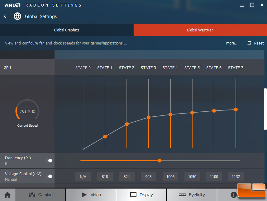
That certainly appears to be the case. I did find a couple of examples of sub 1150mv, but we're only talking 1137mv as the lowest I've found, ATM.
However, this is only judging by Wattman numbers - it may be that the software is pushing the voltage more once you enable manual control.
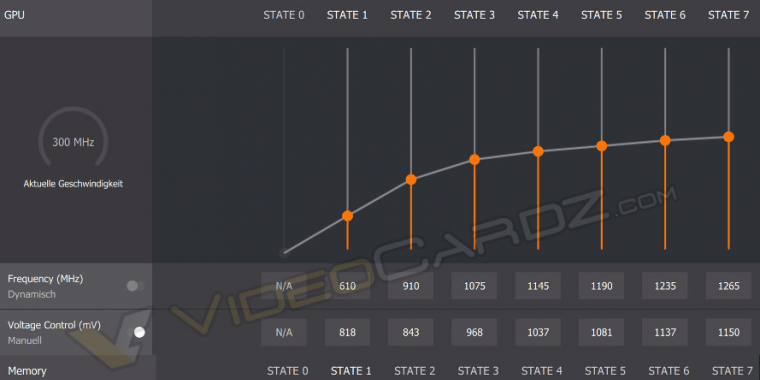
Defaults voltages I've found in Wattman are all pretty much the following:
The only example of a non 1150mv default... and it's still a high 1137mv:
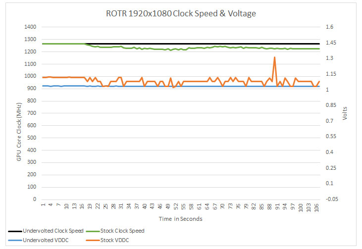
It has been almost universally found that the GPU can run comfortably at 1050mv, many have found 1025 to be stable at stock settings. Under-volting to 1050mv increases performance as well, as the clocks average higher in-game.
LegitReviews reports that default in-game voltage actually began at 1187mv - 37mv higher than the Wattman setting, and it even peaked over 1.3V:
So whatever AMD is doing by default is pretty screwed up.

 :'(
:'(