@Arachnotronic
[TLDR: I found a little gem in a slide from 2015 Investor meeting.]
So I've been looking back to the presentation about SKL-Y vs. A9 from last year, and I noticed something interesting.
http://intelstudios.edgesuite.net/im/2015/archive/wh/archive.html
http://intelstudios.edgesuite.net/im/2015/pdf/2015_InvestorMeeting_Bill_Holt_WEB2.pdf
If you compare slides 17 and 21 (slide 21 is a 2015 update of the slide 17 that they copied from 2013), you will see that
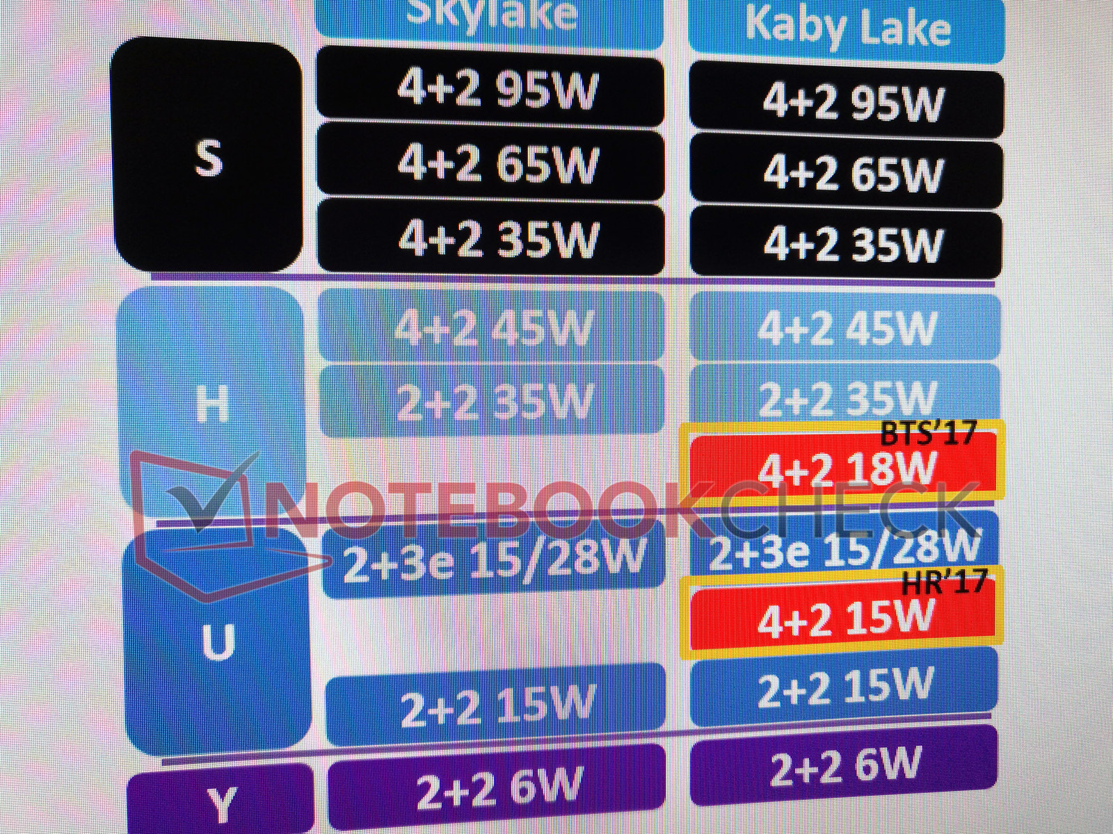
1) At 14nm, Samsung does a bit worse then Intel predicted, so Intel's advantage at 14nm is ever so slightly bigger than they predicted in 2013. (So this talk about 15% higher density was BS, unless A10 uses 16FFC and maybe that does have an increased density.) [
Edit: That is indeed the case, 16FFC has improved density of Apple A10, but TSMC compares 10nm scaling to their 16nm+, so that doesn't matter for the predictions.]
2) For 10nm, Intel predicted that the foundries would be hardly any denser than Intel's 14nm, but their updated version of the graph shows a bigger, quite noticable gap.
3) However, you don't have to be rocket scientist either to see that in the 2013 projection, Intel's forecast of their own 10nm shows that the graph becomes less steep going from 14->10 than from 22->14.
However, in the 2015 slide, you can clearly see that the line remains just as steep, if not even ever so slightly steeper. (We can only guess if this lower 10nm steep in 2013 was done (1) to not give away too much about how much they would shrink at 10nm or (2) if they have since november '13 made their 10nm node more agressive scaling, which might also be plausible because
when they were planning to go to a 3 year cycle, then they would have seen that they had more time to develop 10nm and decided that they could use that to increase density to remain competitive with TSMC and Samsung's agressive node plans.)
On my monitor, I can confirm that the line from 22->14 on the 2013 slide is 22mm, while on the 2015 slide it is 21mm. The 14->10 line drops
vertically 18mm on the 2013 slide and 22mm on the 2015 slide. So this quantitatively confirms my suspicion. BTW, the 32->22 line drops respectively 13mm and 13mm.
For completeness sake, the Samsung line.
2013: 12mm, 5mm and 12mm, for a total of 29mm
2015: 12mm, 3mm and 15mm, for a total of 30mm (So 14/16nm performed less than anticipated, but this does not impact the forecast (which indeed still remains a forecast, since that forecast is based on numbers while the rest of the 2015 graph is based on actual products) of 10nm, on the contrary, the projection has slightly improved.)
And here Intel again in the same format.
2013: 13mm, 22mm and 18mm, for a total of 53mm
2015: 13mm, 21mm and 22mm, for a total of 56mm
Now that I've gone this far into the slide analysis rabbit hole, let's not forget the timing.
Samsung/TSMC, in terms of mm down on the slide.
2012: 0mm (January, AMD HD7xxx series IIRC)
2017: 30mm, for a total of
6mm per year
Same method for Intel.
2010: 0mm (January, Westmere)
2018: 56mm (Canonlake, I round a bit up to calculate in whole years), for a total of
7mm per year
So there you have it guys. Contrary to all the talk, Intel's lead has been growing at 1mm per year in arbitrary units. Or more precise, Intel will have been shrinking 17% more per year, although the comparison is a bit off because Intel's nodes span 8 years while the slide only provides information about Samsung/TSMC for 5 years.
4) This has already been covered by the previous point, but I will say it here again. Even though TSMC and Samsung's 10nm will be reasonably denser than Intel's 14nm, more than previously projected, by 7mm instead of 4mm (So 7mm corresponds to a 1.4x advantage, although I guess you can't simply say that it stacks because then 21mm would be 1.4^3 or 2.7x), Intel's
absolute lead at 10nm will grow thanks to the more aggressive shrinking at 10nm than they previously forecasted: at 14nm Intel is ~10mm ahead of TSMC/Samsung (same as 2013 forecast), while at 10nm Intel will be 15mm ahead (instead of 14mm in 2013 forecast).
So Intel will grow its lead from 10mm to 15mm, even though this time around TSMC and Samsung might have slightly earlier time to market than Intel 14nm vs 20nm, although it remains to be seen if for instance the Galaxy S8 or other Android phones early 2017 will be 10nm, or if it's just the Apple A10X.
In short, if the 2015 graph is accurate, Intel will lead by about 15mm at 10nm, which is more than for instance the 32->22nm node shrink.
Conclusion
So let's face it guys, Intel's not going to lose their manufacturing advantage any time soon. The most a foundry will have shrunk since 2012 is TSMC's 10nm, which is 18mm. So TSMC's 7nm will only be on par with Intel's 10nm at best, and if it launches within 2 years of their 10nm node, you can be sure that it won't shrink 15/18mm. [
Edit: EETimes has since reported
http://www.eetimes.com/document.asp?doc_id=1330503&piddl_msgid=363618 that for 7nm, TSMC claims a "1.63x gate density".]
The only complaint you can have about this analysis is that you have to trust that Intel's done an honest job with this slide. They have done the real analysis and this post is an analysis of an analysis.
I think the most important takeaway for now is that Intel will most likely shrink the interconnect by 0.65x, just like at 14nm (just like they also shrunk the gate pitch by 0.77x like at 14nm), so the interconnect pitch should be 34nm. This is the highest number for the interconnect pitch that I estimated, so this only confirms my previous guess that 10nm would shrink just like 14nm. At this point however, my most optimistic guess of 31nm, seems unlikely (
https://forums.anandtech.com/threads/arm-and-intel-team-up-for-10nm.2483328/#post-38424727).
Edit: I remain with one unanswered question. Since slide 21 is based on actual products, this means that Intel's 14nm advantage (the 21mm) in part comes from other things they have done besides the features shrink. Because in terms of just feature size alone, you would expect a 0.51x shrink at 14nm, but I believe that the line on that slide is based on a higher shrink. When Intel unveiled Broadwell-Y, it became clear that it had in reality a 2.2x increase in density. What I now believe (but this is speculation) is that in reality it might have been even more than that: if Broadwell's die composition changed compared to Haswell to contain more low density cells.
Put another way: we know that the pure silicon has shrunk 0.51x at 14nm, and we know that in reality Broadwell-Y had a 2.2x higher density thanks to other improvements. What we don't know however, is how the composition has changed from Haswell to Broadwell. If Broadwell contains more high density cells, like A9, then that could be the cause of the 2.2x density in part. OTOH, if BDW contains more low density cells, than that might have deflated the actual density improvement, making it look smaller than it actually was. I bet it was the last one, although it's a question by how much that would have changed the picture.
In short, I would have liked to see Haswell thrown onto slide 19 and 20.

")