Discussion Intel Meteor, Arrow, Lunar & Panther Lakes + WCL Discussion Threads

Page 801 - Seeking answers? Join the AnandTech community: where nearly half-a-million members share solutions and discuss the latest tech.

Tigerick

Senior member
Apr 1, 2022
911
829
106
Wildcat Lake (WCL) Preliminary Specs

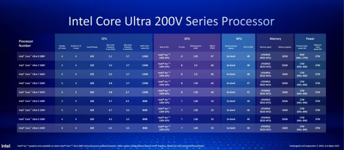
Intel Wildcat Lake (WCL) is upcoming mobile SoC replacing ADL-N. WCL consists of 2 tiles: compute tile and PCD tile. It is true single die consists of CPU, GPU and NPU that is fabbed by 18-A process. Last time I checked, PCD tile is fabbed by TSMC N6 process. They are connected through UCIe, not D2D; a first from Intel. Expecting launching in Q2/Computex 2026. In case people don't remember AlderLake-N, I have created a table below to compare the detail specs of ADL-N and WCL. Just for fun, I am throwing LNL and upcoming Mediatek D9500 SoC.

Intel Alder Lake - NIntel Wildcat LakeIntel Lunar LakeMediatek D9500
Launch DateQ1-2023Q2-2026 ?Q3-2024Q3-2025
ModelIntel N300?Core Ultra 7 268VDimensity 9500 5G
Dies2221
NodeIntel 7 + ?Intel 18-A + TSMC N6TSMC N3B + N6TSMC N3P
CPU8 E-cores2 P-core + 4 LP E-cores4 P-core + 4 LP E-coresC1 1+3+4
Threads8688
Max Clock3.8 GHz?5 GHz
L3 Cache6 MB?12 MB
TDP7 WFanless ?17 WFanless
Memory64-bit LPDDR5-480064-bit LPDDR5-6800 ?128-bit LPDDR5X-853364-bit LPDDR5X-10667
Size16 GB?32 GB24 GB ?
Bandwidth~ 55 GB/s136 GB/s85.6 GB/s
GPUUHD GraphicsArc 140VG1 Ultra
EU / Xe32 EU2 Xe8 Xe12
Max Clock1.25 GHz2 GHz
NPUNA18 TOPS48 TOPS100 TOPS ?


PPT1.jpg
PPT2.jpg
PPT3.jpg


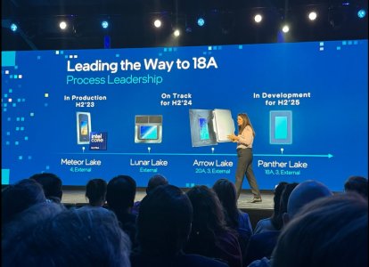
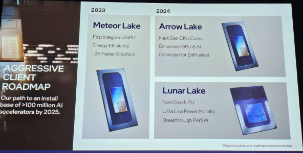
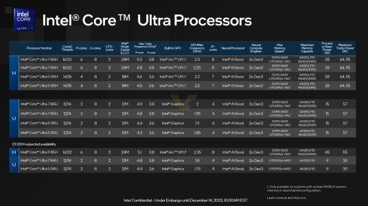
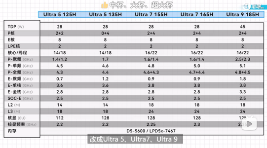
As Hot Chips 34 starting this week, Intel will unveil technical information of upcoming Meteor Lake (MTL) and Arrow Lake (ARL), new generation platform after Raptor Lake. Both MTL and ARL represent new direction which Intel will move to multiple chiplets and combine as one SoC platform.

MTL also represents new compute tile that based on Intel 4 process which is based on EUV lithography, a first from Intel. Intel expects to ship MTL mobile SoC in 2023.

ARL will come after MTL so Intel should be shipping it in 2024, that is what Intel roadmap is telling us. ARL compute tile will be manufactured by Intel 20A process, a first from Intel to use GAA transistors called RibbonFET.


LNL-MX.png
 

Attachments

  • PantherLake.png
    PantherLake.png
    283.5 KB · Views: 24,034
  • LNL.png
    LNL.png
    881.8 KB · Views: 25,527
  • INTEL-CORE-100-ULTRA-METEOR-LAKE-OFFCIAL-SLIDE-2.jpg
    INTEL-CORE-100-ULTRA-METEOR-LAKE-OFFCIAL-SLIDE-2.jpg
    181.4 KB · Views: 72,435
  • Clockspeed.png
    Clockspeed.png
    611.8 KB · Views: 72,321
Last edited:

511

Diamond Member
Jul 12, 2024
5,030
4,533
106
Well no their IP is just not up to snuff.
That's not true tbf if we are talking about Xe3 and beyond but Xe1 was dud and Xe2 improved upon it by very much also by IP I mean the architecture not the physical implementation which sucks big time
 
Last edited:
  • Like
Reactions: Io Magnesso

ondma

Diamond Member
Mar 18, 2018
3,316
1,708
136
My comment was directed specifically at the Gen on Gen performance difference between vanilla non-x3d Zen5 vs. vanilla non-x3d Zen6. There are only three cases where I would expect an X3D parts to be slower in ST performance than it's predecessor or the non-x3d sibling:
1- notable peak clock speed deficit, largely gone with Zen5.
2-Thermal throttling due to heavy MT loads running concurrently or poor cooling leading to heat soak. The vanilla part should generate slightly less thermal load and should maintain slightly higher clocks.
3- a weird corner case that exposes the minor latency hit that the 3d cache causes.

My argument for Zen6 is that, if the rumors are true, the 12 core CCX will have 48MB L3 cache at a comparable latency to the 8 core 32MB L3 CCX in Zen5. The 50% larger L3 would theoretically be available for a pure ST scenario, helping any apps that are dependent on it. It should also be less affected by cache pollution as the cache is larger and has more room to tolerate it with. Add in the expected 10% pic improvement from the rumor slide and it should be able to best Arrow Lake too.
I am not a chip designer, so this is a legitimate question, not a criticism. Which is more important, the absolute amount of cache, or the cache per core? I ask this because even though the proposed Zen 6 CCD has 50% more cache, it also has 50% more cores, so the cache per core is 4MB in both configurations.
 

Kepler_L2

Golden Member
Sep 6, 2020
1,039
4,444
136
I am not a chip designer, so this is a legitimate question, not a criticism. Which is more important, the absolute amount of cache, or the cache per core? I ask this because even though the proposed Zen 6 CCD has 50% more cache, it also has 50% more cores, so the cache per core is 4MB in both configurations.
You can look at Zen2 vs Zen3, both had 32MB L3 but on Zen2 only 16MB were available for each core due to split CCX design.
 

adroc_thurston

Diamond Member
Jul 2, 2023
7,812
10,530
106
I am not a chip designer, so this is a legitimate question, not a criticism. Which is more important, the absolute amount of cache, or the cache per core? I ask this because even though the proposed Zen 6 CCD has 50% more cache, it also has 50% more cores, so the cache per core is 4MB in both configurations.
You want more cache in general for 1T or gaming, and more cache per core for anything nT.
Venice-D goes to 4M L3@core despite a generational membw bump for a reason.
 

dangerman1337

Senior member
Sep 16, 2010
411
57
91
as long as it offers the best gaming performance it is gonna sell 30-35mm2 extra die will be worth it
Hopefully they do it P Core Only, imagine 12 or more Griffin Cove Cores with RZL-S with all that extra cache and crazy fast DDR5 with low latency? Insane gaming performance.
 

DavidC1

Platinum Member
Dec 29, 2023
2,006
3,153
96
Why is it not that's1MB increase for 1 Cycle Skymont is 19 Cycles 4MB L2.
Latency is also affected by design choices, so you can't compare 1:1 with Skymont, which is lower power, and is also a shared cache for 4x cores.

1 cycle increase for mere 33% capacity increase is nothing good. Even if latency stayed the same, I wouldn't call it impressive, and actually even against Skymont it's just 1 cycle reduction. You'd think a "performance" focused core in 2027 would be better than E core in 2025.

The last Intel core with impressive cache structure was Sandy Bridge. It could overclock to 4.5GHz, the cache was at same clock as the core, and at 8MB capacity had 25 cycle latency, despite being an L3 cache. I wonder how it would fare with 18A?
If only they weren't a bunch of idiot in Intel DC GPU space not cancelling everything.
That's cause they weren't selling. Lot of vendors were on board with mobile ARC GPUs until it found the perf/W was bad and the drivers were atrocious. The last famous Intel DC GPU was Ponte Vecchio, which had enormously complicated packaging that made Lunarlake's MoP complaint like it added a penny to BoM and was maybe 20% faster in cornercase scenarios.

The last JPR dGPU marketshare showed Intel isn't even blip in the radar now. They are 0% according to them. Probably sold few thousands to low tens of thousands. The best case is 0.49%, since numbers are rounded down.
 
Last edited:

511

Diamond Member
Jul 12, 2024
5,030
4,533
106
Latency is also affected by design choices, so you can't compare 1:1 with Skymont, which is lower power, and is also a shared cache for 4x cores.

1 cycle increase for mere 33% capacity increase is nothing good. Even if latency stayed the same, I wouldn't call it impressive, and actually even against Skymont it's just 1 cycle reduction. You'd think a "performance" focused core in 2027 would be better than E core in 2025.
It's good tbh also it's shares between 2 cores as well also bout the P core vs E core in terms of IPC I would think that P and E core have similar IPC by H2 26 when Nova Lake launches.
The last Intel core with impressive cache structure was Sandy Bridge. It could overclock to 4.5GHz, the cache was at same clock as the core, and at 8MB capacity had 25 cycle latency, despite being an L3 cache. I wonder how it would fare with 18A?
8 MB at 25 Cycle is pretty Good I wonder what's the Cycles will be for NVL L3 anything under 50 would be Good imo.
That's cause they weren't selling. Lot of vendors were on board with mobile ARC GPUs until it found the perf/W was bad and the drivers were atrocious. The last famous Intel DC GPU was Ponte Vecchio, which had enormously complicated packaging that made Lunarlake's MoP complaint like it added a penny to BoM and was maybe 20% faster in cornercase scenarios.
Not to mention ARC has been delayed so much.
The last JPR dGPU marketshare showed Intel isn't even blip in the radar now. They are 0% according to them. Probably sold few thousands to low tens of thousands. The best case is 0.49%, since numbers are rounded down.
Well maybe they already shipped in Q4 25 when they were 1% and after that low shipments.
 
  • Like
Reactions: Io Magnesso

DavidC1

Platinum Member
Dec 29, 2023
2,006
3,153
96
It's good tbh also it's shares between 2 cores as well also bout the P core vs E core in terms of IPC I would think that P and E core have similar IPC by H2 26 when Nova Lake launches.
In Sandy Bridge, it went from 41 cycles to 25 cycles, nearly a 40% reduction, while clocking much higher in the new Turbo mode consistently as well.

They aren't losing money on ARC because of high BoM, that is nonsense. They are losing money on ARC because basically there's no volume. They could have $50 BoM and it would still lose them money.
 
Last edited:
  • Like
Reactions: MoistOintment

AcrosTinus

Senior member
Jun 23, 2024
221
226
76
Yeah but not anymore going forward the private alley is going away 2P people have to share 😂.


If only they weren't a bunch of idiot in Intel DC GPU space not cancelling everything.


Why is it not that's1MB increase for 1 Cycle Skymont is 19 Cycles 4MB L2.

Their Heydey died with 10nm delays lol.
I have a feeling that this is the secret on how they were able to increase the P-core count. Instead of having a stop per P-Core and E-Core cluster, 2P-Cores share a stop and maybe even the E-Core cluster is now 8 cores big. This sounds more realistic to me than two compute dies with two separated ring-buses? with each having 12stops.

Could also be a way to reduce the stops per ring to 8, essentially having 16 stops if two dies are really employed in nova.
 
  • Like
Reactions: Io Magnesso

511

Diamond Member
Jul 12, 2024
5,030
4,533
106
In Sandy Bridge, it went from 41 cycles to 25 cycles, nearly a 40% reduction, while clocking much higher in the new Turbo mode consistently as well.
Didn't know that it is insane improvement lol.
They aren't losing money on ARC because of high BoM, that is nonsense. They are losing money on ARC because basically there's no volume. They could have $50 BoM and it would still lose them money.
Yes but I think the volume they are using now is due to the prepayment they did for Arc.
I have a feeling that this is the secret on how they were able to increase the P-core count. Instead of having a stop per P-Core and E-Core cluster, 2P-Cores share a stop and maybe even the E-Core cluster is now 8 cores big. This sounds more realistic to me than two compute dies with two separated ring-buses? with each having 12stops.
Yes also I doubt 8E core cluster 12 -> 8 is a good amount of reduction for cores in Ring.
Could also be a way to reduce the stops per ring to 8, essentially having 16 stops if two dies are really employed in nova.
Each die has separate ring and they are connecting using some shared fabric.
 
  • Like
Reactions: AcrosTinus

DavidC1

Platinum Member
Dec 29, 2023
2,006
3,153
96
Could also be a way to reduce the stops per ring to 8, essentially having 16 stops if two dies are really employed in nova.
And AMD doesn't have this problem. An engineering-issue, or should I say lack of it? Oh right, cause they lack engineers. Back to crossbar, or rethought of mesh, do something new. The 2011 Sandy Bridge design is showing it's age very much.
Didn't know that it is insane improvement lol.
Yes, that is due to the Ring, which was well thought out and novel design. They regressed every gen since then. Their fabric has also been mediocre at best since. Which are details that are lost when you have brain drain.

They want to give up their Networking/WiFi division now? What is on their minds?
 

Io Magnesso

Senior member
Jun 12, 2025
578
165
71
And AMD doesn't have this problem. An engineering-issue, or should I say lack of it? Oh right, cause they lack engineers. Back to crossbar, or rethought of mesh, do something new. The 2011 Sandy Bridge design is showing it's age very much.

Yes, that is due to the Ring, which was well thought out and novel design. They regressed every gen since then. Their fabric has also been mediocre at best since. Which are details that are lost when you have brain drain.

They want to give up their Networking/WiFi division now? What is on their minds?
There are rumors that the NEX division will be given up, but the network/wifi I don't think it's possible to let go
I think that the dismantling of the NEX division will be merely a change of personnel within the Intel company.
 

AcrosTinus

Senior member
Jun 23, 2024
221
226
76
And AMD doesn't have this problem. An engineering-issue, or should I say lack of it? Oh right, cause they lack engineers. Back to crossbar, or rethought of mesh, do something new. The 2011 Sandy Bridge design is showing it's age very much.

Yes, that is due to the Ring, which was well thought out and novel design. They regressed every gen since then. Their fabric has also been mediocre at best since. Which are details that are lost when you have brain drain.

They want to give up their Networking/WiFi division now? What is on their minds?
That is true, Intel introduced the mesh in HEDT and benchmarks show that if clocked high enough the penalty compared to the ring are minimal but the scaling it vastly superior. Had they invested some time in a mainstream variant, the mesh could have been vastly more performant but who knows....

AMD being on a mesh is news to me, this explains the sub 20ns core to core latency within a CCD.
 

Doug S

Diamond Member
Feb 8, 2020
3,730
6,593
136
I am not a chip designer, so this is a legitimate question, not a criticism. Which is more important, the absolute amount of cache, or the cache per core? I ask this because even though the proposed Zen 6 CCD has 50% more cache, it also has 50% more cores, so the cache per core is 4MB in both configurations.

It is the same cache per core only if you use all cores.

In the world most of us occupy our CPUs are typically loading only a few cores at a time so you get more cache per core in those circumstances. But even if you're the outlier who is often running all cores at 100% you aren't any worse off than before and now you have 50% more cores for your outlier tasks.
 

Thibsie

Golden Member
Apr 25, 2017
1,149
1,353
136
It is the same cache per core only if you use all cores.

In the world most of us occupy our CPUs are typically loading only a few cores at a time so you get more cache per core in those circumstances. But even if you're the outlier who is often running all cores at 100% you aren't any worse off than before and now you have 50% more cores for your outlier tasks.

Yeah, but might thread 'eat' the second core cache ? I mean, both core will compte for cache then, no ?
Also, more read/write ports could slow cache access (speed/latency) or augment complexity ?
This might be completely false, I dunno much about cache workings.