It is the curse of Tejas that put Intel in its current predicament. They really should go back and modernize Tejas for a modern node. Until they do that, they will keep running into hurdles. An unjust deed never goes unpunished.
They will probably have to fab at GlobalFoundries. Modified it from the research papers regarding heat on high-performance GAA/Shrinked BOX FDSOI:

Consider it a range(12FDX actual might be between 22FDX/12FDX and GAA between FinFET/GAA), also made it in like 5 seconds, so pardon the weird GAA tail/head angle and 12FDX tail being higher than 22FDX.
12FDX tensile Si NFET+compressive SiGe PFET and BOX=15nm(eSoC3) and lower BOX=10nm(eSoC3+).
I expect only RISC-V cores will push speeddemon to get around high-cost per-density FinFETs/GAA. Which immediately cuts out Intel since they will want x86.
Can take a scalar-core with RISC-V to 10 GHz to 20 GHz and it would still be viable against density-focused Fin/GAA.
2x 64-bit ALUs
2x 64-bit AGUs
2x 64-bit FPUs (non-SIMD)
Low-cost speed demon = dual-core replacing four-core/eight-core designs // 8-core tablets that are just a slow in-order cores or anemic OoO+many InO.
High-cost speed demon = octo-core replacing 32-core/64-core designs. // 64-core E2/E-next products that are relatively slow, where the market is FAST transaction rates.
Investment into Speeddemon architectures are only viable if there is big leaps in memory throughput.
RAM:
DDR2/DDR3/DDR4 DIMM, low speed delta
LPDDR5/LPDDR6/+ LPCAMM,
high speed delta
Read mostly memory:
HDD/Slow Flash SATA, low speed delta
PCIe5/PCIe6/+ SLC+xLC low-latency/high-throughput NVMe,
high speed delta
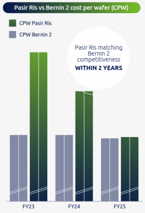
There is also Nantero's NRAM that can be used in RAM/RMM. What they are showing to the USG is pretty fast. Of, this I doubt Europe or Singapore would bother with Ultra-High-Freq. So, it would largely be up to Fab8 getting cheap 300mm FDSOI (from pasir ris) to get 12FDX out. In which, USG can fund these crazy speeddemon nutjobs with a science act.

FY25 = Late 2024
In short:
FinFET -> GAA -> Complementary GAA => High Density/High IPC preference for high performance.
FDSOI -> Planar Gate-semi-around -> Wafer M3D PGSA => High Speed/Mid IPC preference for high performance.
Coming out with a design that continues this trend requires FDSOI. It is unlikely to occur with FinFET/GAA/CGAA:

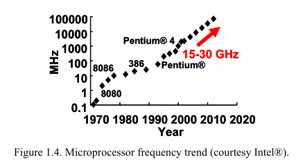
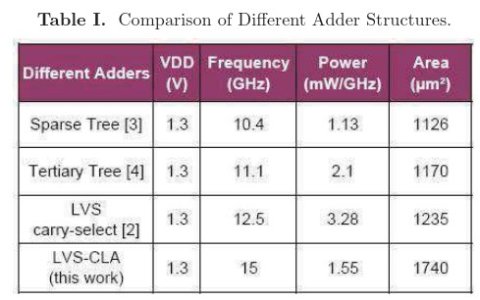
Last major work, with Pentium 4-esque design had 15 GHz in target.
[3] = "A 9-GHz 65-nm Intel® Pentium 4 Processor Integer Execution Unit"

Also, while the CPU is at
https://valid.x86.fr/show_oc.php?id=2676347 , 8352.86 MHz (334.11 * 25) isn't the Fast ALUs in the Integer Core running double? [16705.72 MHz]
Almost every aspect of the Integer core is 2x processor clock. Ex: "The 144-entry 6r3w register file (Fig. 5.7.6) uses the 2× frequency clock to obtain a throughput of 12r6w per processor clock."
Before 65-nm Intel Pentium 4 came out in IEEE 2006 came out rewind to TeraHertz/"Pentium 5" target node 2002:

The people who need to know do know. A true proper Tejas can only be on a FDSOI node.
Some delicious quotes:
"Intel denied that it's behind its rivals, claiming that it will skip traditional SOI and move to a next-generation technology called “thin SOI” or fully-depleted SOI"
"We expect to fully deploy the TeraHertz transistor by the second half of this decade. - Intel"


