witeken
Diamond Member
I would've posted those of course. Here are all the sessions: https://intel.activeevents.com/sf14/connect/search.ww
So, how many fins does one schematic transistor consist of, on average? I think it's quite high since Mark Bohr said transistors are often made with 2 and 3 or 4 fins and William Holt said it's very uncommon to use 1 or even 2 fins, so wouldn't that mean that if Broadwell on average has 2 fins per schematic transistor, that the apples to Apples comparison would be (in this fictional case) 2.6B transistor for Core M vs 2.0B for A8?Wow, this schematic vs layout vs fin count is intense. Fin count is no different from layout count at the end of the day. However the amount that fin/layout count differs from schematic count is higher on a finfet process (assuming iso-performance). Planar transistor can vary its width without counting as a new layout transistor up to a certain point. Finfets, without being able to vary the height of a fin, you can only add more fins.
So, how many fins does one schematic transistor consist of, on average?
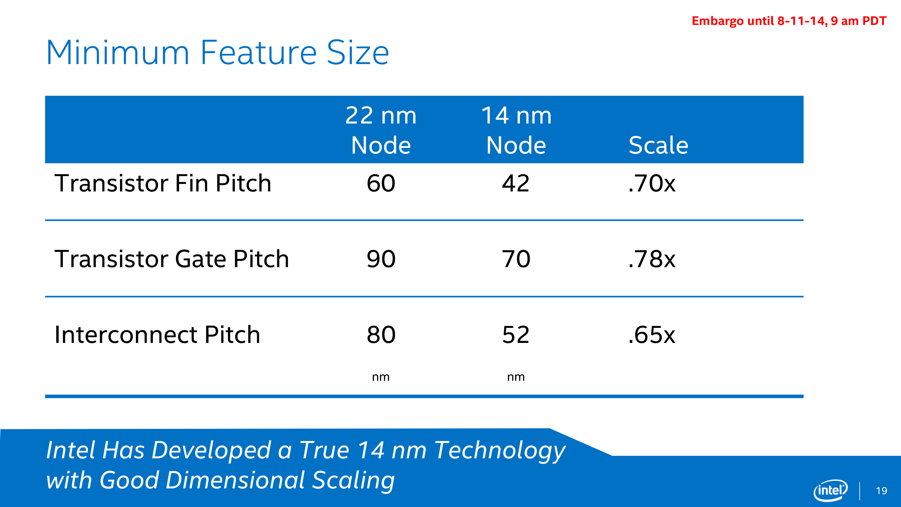
Mark Bohr said the 14nm process has a 0.51x neutral density scaling, but the real density scaling is 2.2x (0.45x), so is that difference caused by reduction of fins?
Okay, any less detailed information you care to share?I would tell you, except I would need to hire you first. 😛
If you take the transistor estimate (gate*interconnect) and compare it with 22nm, you get a 0.51x scaling, but if you look in the real world, Core M has a 2.2x higher density than Haswell-Y:I didn't see this quote but it could be several things. Better current/um could improve density as you don't need as large of a transistor to achieve the drive strength you need. Or is he talk about w/ features vs w/o features.

2.2x scaling: http://intelstudios.edgesuite.net/im/2014/pdf/2014_Intel_IM_Holt.pdf page 21
BTW, fast reply. (although I'd rather have a slower but more informative answer)
BTW, fast reply. (although I'd rather have a slower but more informative answer)
The 2.2x area reduction looks like the final result so you can't isolate it to one variable. The improved transistor drive strength helps, but design methodology and design choices can also lead to that 2.2x reduction.
So the reduction in fins per transistor is negligible, as opposed to what Bohr and Holt have been saying?
Now that I figured you work for Intel, I should try and ask what you are working on? Also, have you ever heard of something called Icelake?It's definitely not negligible, it's quite significant. I just want to get some credit too. 😛
If I remember correctly, Dave's a uarch guy.Now that I figured you work for Intel, I should try and ask what you are working on? Also, have you ever heard of something called Icelake?
Now that I figured you work for Intel, I should try and ask what you are working on? Also, have you ever heard of something called Icelake?
I can do my best to answer academic questions. So if you want to know what's a schematic, what's layout, what's in a CPU, <insert generic engineering question here>, I'll be glad to help out. But I generally abstain from anything specific to my work. Sorry!
I already saw that when I just (re)read a whole bunch of your posts. But I tried.
Then what do you work on if we ignore code names?
Multiple at once?
Is it a Tick, or a Tock?