Discussion Intel current and future Lakes & Rapids thread

Page 791 - Seeking answers? Join the AnandTech community: where nearly half-a-million members share solutions and discuss the latest tech.

IntelUser2000

Elite Member
Oct 14, 2003
8,686
3,785
136
I'm going off Raichu's spec 2017? 2007? testing for IPC.
In Libx264 testing by ChipsandCheese, IPC for gracemont was ~75% of GLC. I believe he used a 12900k.
Gracemont's chief architect claims it has greater than skylake level INT IPC as well.
Can't find any more IPC testing of gracemont. From what I have seen, IPC difference for gracemont isn't as bad as 40-50%.
Vector performance is also a lot more commonplace in the server market IIRC.
When he says it's better, he's talking about 5%. Also they just said with Raptorlake release the 2-4% improvement with prefetcher and cache changes finally got it to Skylake level. Obviously even Skylake has 2x vector performance so they aren't talking about that.

Vector performance only matters in the HPC market. Rest of server is integer. Cloud services, Enterprise, web servers.

Also Intel's talking about wide range of applications, not just one single benchmark. It's 40-50% just based on their own claims, which many benchmarks prove.

Real client vector code is a fraction of the total thing. Doubling that won't get you more than 5-10%. I challenge you to find client benchmarks that show big differences with AVX. You can see from Skylake-X benchmarks that you can find maybe 1-2 benchmarks. Anand's only test that shows a big gain is pretty much synthetic code that Ian himself coded.
 
Last edited:

Geddagod

Golden Member
Dec 28, 2021
1,147
1,003
106
I think that reference probably predated Crestmont's addition to the roadmap. But let's say Crestmont is smaller, maybe around 10%, and then a big 20% jump with Skymont in 2024, and then a tick Darkmont(?) for 10% in 2025...

Even if those numbers wind up being off, which they probably will, it's quite plausible that Intel will have a RWC-class IPC Atom core in 2025. Add in a full node advantage, and I could totally see it being an upgrade over even GNR at a server operating point. And if DMR isn't coming till 2026, it better have more than just Lion Cove. That won't be competitive if released midway between Zen 6 and 7.
Those numbers would put it at ~15% better INT IPC and ~90% of the FP IPC of GLC. Not bad, INT wise it would prob be comparable to RWC+ and might even be not far off from LNC lmao. I think that guess is a bit optimistic though.
ST might still be a sticking point for GNR. But I think there may be a point that CLF might be a complete upgrade over GNR.
LNC is on TSMC 3nm/Intel 20A. I would be surprised if at the very least we don't see a LNC+ in DMR, if not Panther Cove itself to match it's Intel 18A node and 2026 time frame.
I would suspect a early 2026 launch wouldn't put it in too bad of a timeframe vs Turin though. Turin I think could launch midway in 2024, so Zen 6 server would prob be near the tail end of 2025. Early 2026 would mean ~1H time frame.
 

Geddagod

Golden Member
Dec 28, 2021
1,147
1,003
106
When he says it's better, he's talking about 5%. Also they just said with Raptorlake release the 2-4% improvement with prefetcher and cache changes finally got it to Skylake level. Obviously even Skylake has 2x vector performance so they aren't talking about that.

Vector performance only matters in the HPC market. Rest of server is integer. Cloud services, Enterprise, web servers.

Also Intel's talking about wide range of applications, not just one single benchmark. It's 40-50% just based on their own claims, which many benchmarks prove.

Real client vector code is a fraction of the total thing. Doubling that won't get you more than 5-10%.
I mean I agree that better prob means 5%
When did they say with RPL's release that prefetcher and cache changes got gracemont+ to SKL level?
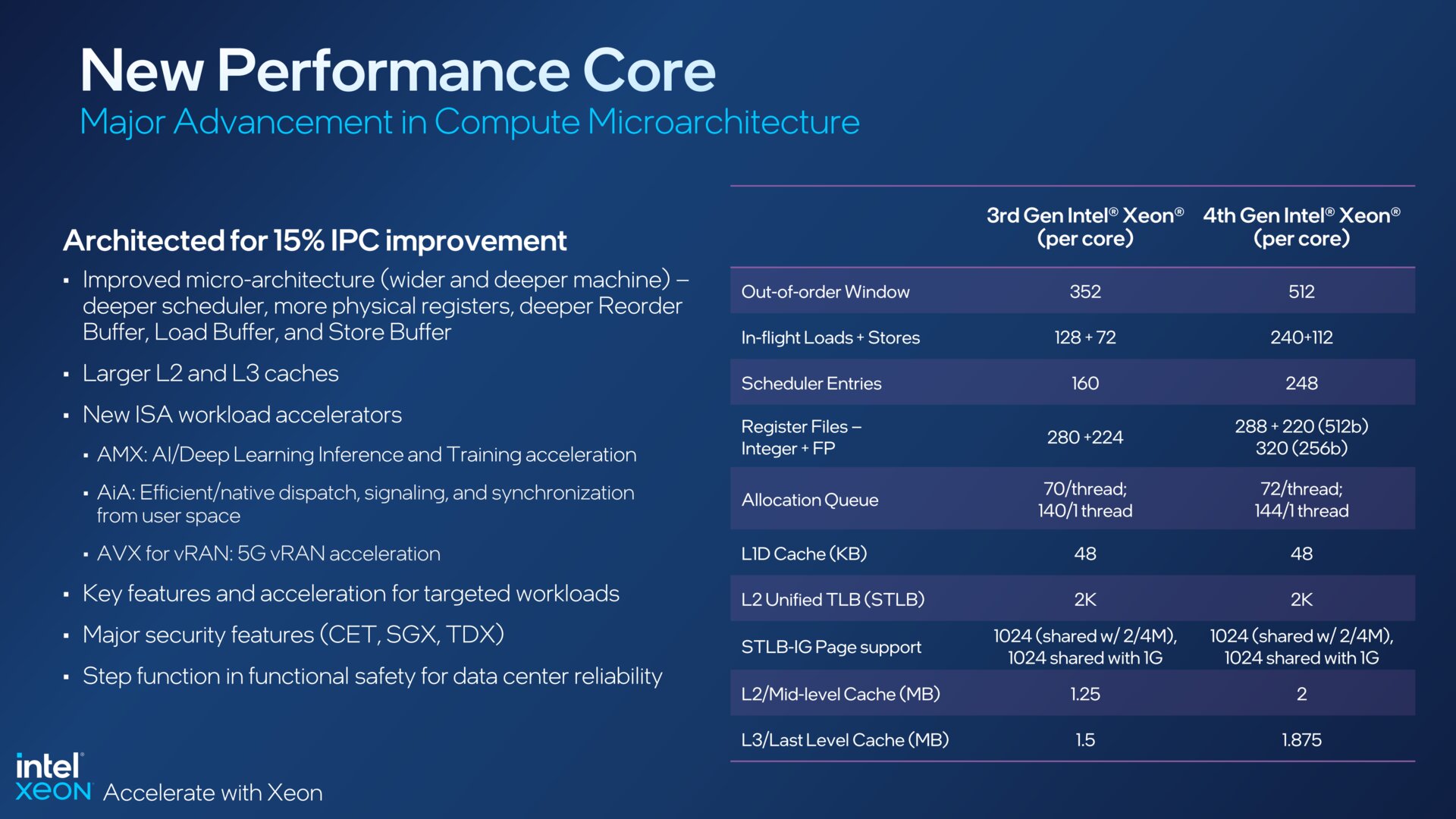
Intel always claimed gracemont was SKL level. Sunny Cove was a 18% IPC increase over SKL, but GLC wasn't a 19% IPC improvement over Sunny Cove. It was a 19% improvement over Cypress Cove.
Intel claims GLC is a 15% improvement over Sunny Cove.
FmMRUmWaAAM4O2s


If we assume SKL/Gracemont has 1IPC, that would put GLC at 1 x 1.15 (GLC vs SNC) x 1.18 (SNC vs SKL) = 1.36.
This would mean Gracemont has 1/1.36 = ~75% the IPC of GLC.
This is also supported by Raichu's SPEC testing, which is industry standard, and also Chips and Cheese testing. You mention that the IPC testing showing Gracemont to be only 40-50% the IPC of the big core is supported by "many benchmarks" but I have only found those two cases of IPC testing online. Perhaps you can show me your benchmarks?
I don't think I did any of my math wrong either, so I am confused how we are using pretty much the same data but came up with such different results.
 

Geddagod

Golden Member
Dec 28, 2021
1,147
1,003
106
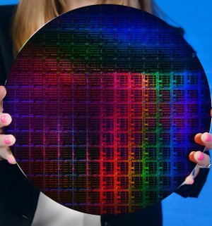
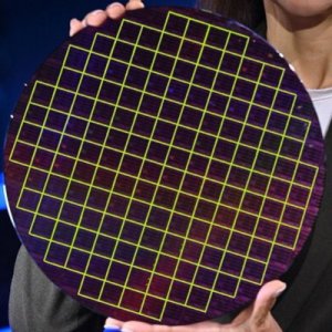
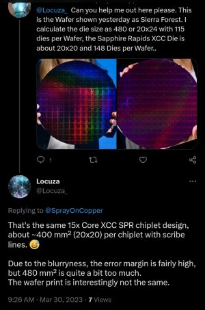
This is what I was able to calculate based on High Resolution Wafer Shot of Sierra Forest Compute die.

About 480 mm^2 and 115 fully printed Dies

View attachment 78820

View attachment 78821
The size of that die makes it seem like Intel expects Intel 3 to be yielding like Intel 7 essentially. Smaller chiplets would probably safeguard them for if Intel 3 faces yield issues.
Something about the math of this just isn't clicking for me though.
If 4E-cores take up the space of 1P core, and just 96 E-cores take up ~480mm^2.... 24 P cores would take up the space of 480mm^2? 44P-cores would be pretty much reticle limit no?
What's worse about this estimation is the fact that a server P-core is likely to take up even more than 4E-cores worth of space. Yes Sierra Glenn apparently has more L2 cache, but P-on client vs server have an extra addition to the FP block, the AMX extension, adding on a mesh stop, etc etc
 
  • Like
Reactions: A///

A///

Diamond Member
Feb 24, 2017
4,352
3,154
136
Your math is right. I did it myself today at work while chugging back on coffee and donuts. I had a looksie on the web and saw others were coming to the same conclusion. Either Intel has a card up their sleeve or have shrunk their e cores more. Sometimes Intel's own claims give north korea a run for their money.
 
  • Haha
Reactions: Geddagod

witeken

Diamond Member
Dec 25, 2013
3,899
193
106
Being Optimistic here, Intel can harvest 148 fully printed dies per wafer on SPR-SP, 15 cores per die is about 2220 Cores per Wafer.
View attachment 78803

On Emerald Rapids the math is: 68 fully printed dies and 34 cores per die is 2318 cores per 300 mm wafer.
View attachment 78804

That's only 4% Higher cores printed in favor of the two large die per CPU Aproach, which is insignificant but yields should be Higher on the smaller dies as defects become a mayor issue the larger the printed die is

oooh this is tough lol. Looks like a 6X4 grid IMO. Either way I don't think this is the full SRF compute tile... right?

Yeah looks like 6x4 to me as well, its just one compute die, there will be two of those on the SP Variant.

This can't be right. There's only 1 compute die in Sierra Forest-SP.

 
Last edited:

A///

Diamond Member
Feb 24, 2017
4,352
3,154
136
I'm of the mindset that hearing more about later future platforms and progress being made on them meaning intel is on track and doing it right. I could be wrong but I hope not.
 

A///

Diamond Member
Feb 24, 2017
4,352
3,154
136
I mean I agree that better prob means 5%
When did they say with RPL's release that prefetcher and cache changes got gracemont+ to SKL level?
Intel always claimed gracemont was SKL level. Sunny Cove was a 18% IPC increase over SKL, but GLC wasn't a 19% IPC improvement over Sunny Cove. It was a 19% improvement over Cypress Cove.
Intel claims GLC is a 15% improvement over Sunny Cove.
FmMRUmWaAAM4O2s


If we assume SKL/Gracemont has 1IPC, that would put GLC at 1 x 1.15 (GLC vs SNC) x 1.18 (SNC vs SKL) = 1.36.
This would mean Gracemont has 1/1.36 = ~75% the IPC of GLC.
This is also supported by Raichu's SPEC testing, which is industry standard, and also Chips and Cheese testing. You mention that the IPC testing showing Gracemont to be only 40-50% the IPC of the big core is supported by "many benchmarks" but I have only found those two cases of IPC testing online. Perhaps you can show me your benchmarks?
I don't think I did any of my math wrong either, so I am confused how we are using pretty much the same data but came up with such different results.
do you happen to have an updated or new slide for xeons using lion coves core design?
 

nicalandia

Diamond Member
Jan 10, 2019
3,330
5,281
136
Apparently it's SPR XCC
No chance, the die size on the Wafer Shown is 480 mm^2 and only up to 115 Fully printed dies can be Harvested. The SPR-SP XCC die is smaller at 400 mm^2 And up to 148 dies can be harvested.

Sierra Forest Wafer
SierraForestWaferX-itB2au-uZ-transformed.jpeg

SPR XCC Wafer
Fc0U-lYX0AAG6Q7.jpeg
Do the math.
 
Last edited:
  • Like
Reactions: Geddagod

mikk

Diamond Member
May 15, 2012
4,112
2,106
136
No chance, the die size on the Wafer Shown is 480 mm^2 and only up to 115 Fully printed dies can be Harvested. The SPR-SP XCC die is smaller at 400 mm^2 And up to 148 dies can be harvested.


It is SPR-SP XCC, you can see it from the picture. There are 15 CPU cores and the memory control tile. Sierra Forest is a single tile chip. Maybe your die size claims are off.
 

nicalandia

Diamond Member
Jan 10, 2019
3,330
5,281
136
It is SPR-SP XCC, you can see it from the picture. There are 15 CPU cores and the memory control tile. Sierra Forest is a single tile chip. Maybe your die size claims are off.
Just look at the Wafer, Sapphire Rapids XCC Wafer shows 15 rows, the Sierra Forest Wafer shows 14 because the die is not a simple square like Sapphire Rapids which is a simple 20x20 square. The Sierra Forest is a longer die a 20x24.

I took the time and downloaded the Higher Res Die Shot.
 

nicalandia

Diamond Member
Jan 10, 2019
3,330
5,281
136
I asked Locuza about it, he thinks its old Sapphire Rapids XCC, interestingly enough the Print is different as in less efficient than the Original old design perhaps its an entirely different CPU? I guess they did not have finished wafers as they expected?

Screenshot_20230330-111955_Chrome.jpg
 
  • Like
Reactions: moinmoin

H433x0n

Senior member
Mar 15, 2023
846
894
96
I’ve got a question for some of the OGs of this forum.

When they show off a wafer like this.. it’s pretty much trashed right? Do they select a random engineering sample wafer that had bad yields for these press images? So by doing this, they’re really only sacrificing ~20-30 engineering sample CPUs?
 

Geddagod

Golden Member
Dec 28, 2021
1,147
1,003
106
I asked Locuza about it, he thinks its old Sapphire Rapids XCC, interestingly enough the Print is different as in less efficient than the Original old design perhaps its an entirely different CPU? I guess they did not have finished wafers as they expected?

View attachment 78842
I'm sure if someone like Ian Cutress or another established journalist asks Intel, they would clarify on if they made a mistake on the wafer labelling or not.
 

Exist50

Platinum Member
Aug 18, 2016
2,445
3,043
136
I’ve got a question for some of the OGs of this forum.

When they show off a wafer like this.. it’s pretty much trashed right? Do they select a random engineering sample wafer that had bad yields for these press images? So by doing this, they’re really only sacrificing ~20-30 engineering sample CPUs?
Yeah, that wafer is just a prop now. They wouldn't even necessarily test it for yields first. Not sure about the specifics of their wafer handling flow, but it might be easier to just pluck it from the line before all that testing.

Though I remember reading of one example from many, many years ago when Intel had a single, perfect wafer, and they ended up framing it for the CEO.