Their HEDT segment is dead. It's called Xeon Workstation now.
This new CPU Xeon W-3433 is the natural successor to the Ice lake Xeon W-3335(16 core also) which lags behind the Zen2 3955WX. This new W-3433 might be a good match for the 5955WX but will be No match for the 7950WX
View attachment 63337
View attachment 63338
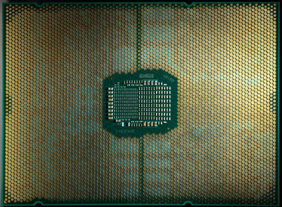
Intel Sapphire Rapids Xeon W5-3433 'Fishhawk Falls' HEDT Workstation CPU Spotted: 16 Golden Cove Cores, 32 Threads & 45 MB L3 Cache
Intel's Sapphire Rapids Xeon-W CPU, the W5-3433, which is designed for the HEDT Fishhawk Falls workstation platform has been spotted.wccftech.com
at only 16 cores it could probably clock high enough to come close to 7950x in performance.
edit: misread 7950wx as 7950x, my bad. Still, 16 core Zen4 product, only TR one, right?
