-
We’re currently investigating an issue related to the forum theme and styling that is impacting page layout and visual formatting. The problem has been identified, and we are actively working on a resolution. There is no impact to user data or functionality, this is strictly a front-end display issue. We’ll post an update once the fix has been deployed. Thanks for your patience while we get this sorted.
You are using an out of date browser. It may not display this or other websites correctly.
You should upgrade or use an alternative browser.
You should upgrade or use an alternative browser.
Discussion Intel current and future Lakes & Rapids thread
Page 571 - Seeking answers? Join the AnandTech community: where nearly half-a-million members share solutions and discuss the latest tech.
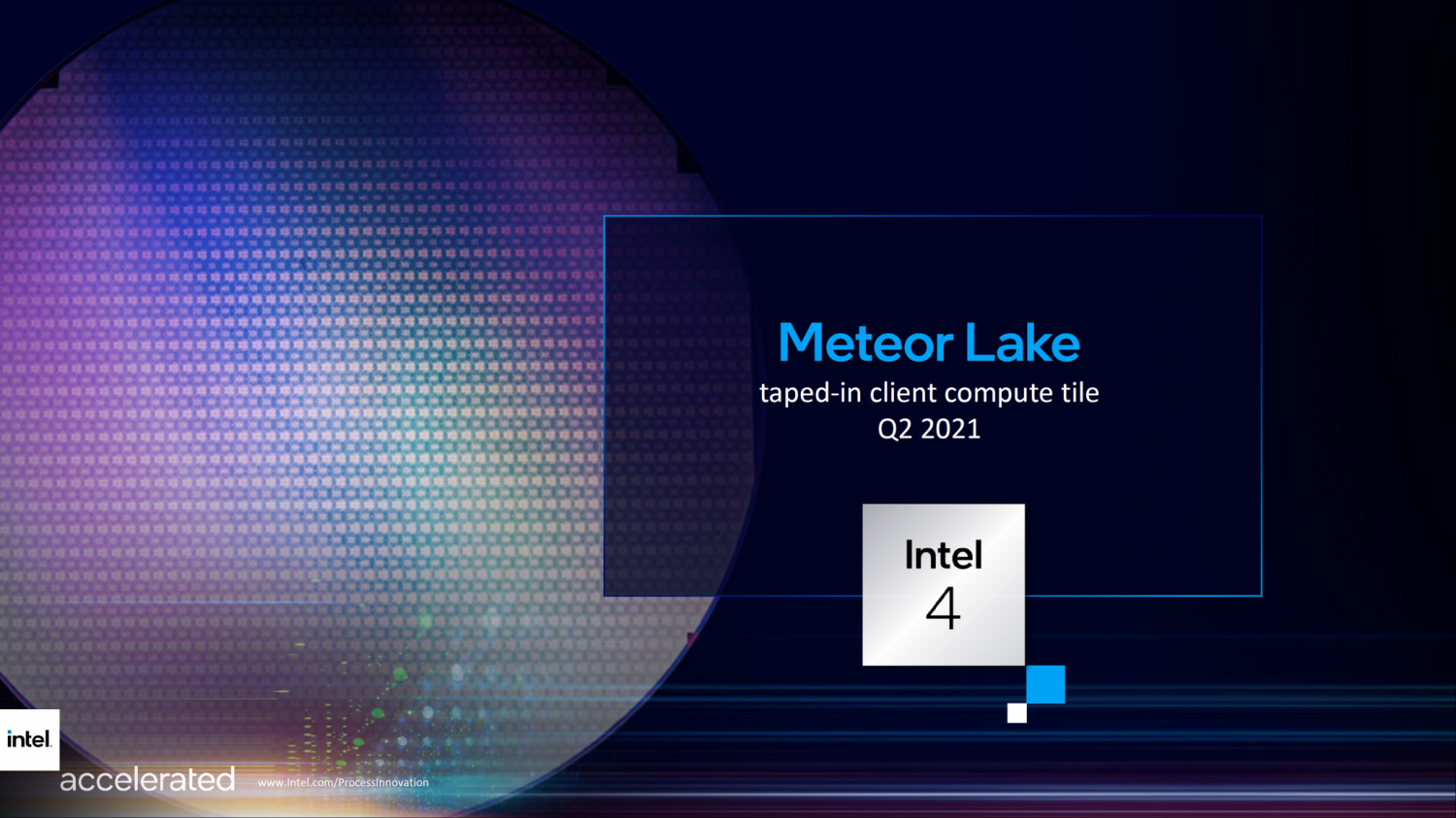
Who is the audience for this article? I assume the technologically ignorant.CNET posted a pretty cool article where they toured Intel's Arizona fab and they nabbed a few photos of Intel's future products, including Meteorlake:
This says it all.
"Intel has lagged TSMC and Samsung overall, but it's ahead with an increasingly important technology: chip packaging that lets Intel make a single processor out of multiple chip elements, variously called tiles, chiplets or dies."
Saylick
Diamond Member
Yeah, it's basically a PR piece for Intel to allow them to say "Look at what we're doing! We're not behind!"Who is the audience for this article? I assume the technologically ignorant.
This says it all.
"Intel has lagged TSMC and Samsung overall, but it's ahead with an increasingly important technology: chip packaging that lets Intel make a single processor out of multiple chip elements, variously called tiles, chiplets or dies."
dullard
Elite Member
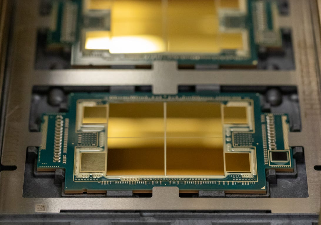
Forgive me if I'm wrong here, since I don't know much about memory chips, but aren't the HBM connections central to the chip? Meaning that the gaps have to be wide?Interesting to see how big the gaps between EMIB endpoints appear to be, especially those for the HBM. That's a lot of area to cut out from the substrate.
https://en.wikipedia.org/wiki/High_...301-DSC10363_-_ZS-retouched_(29514443756).jpg
Saylick
Diamond Member
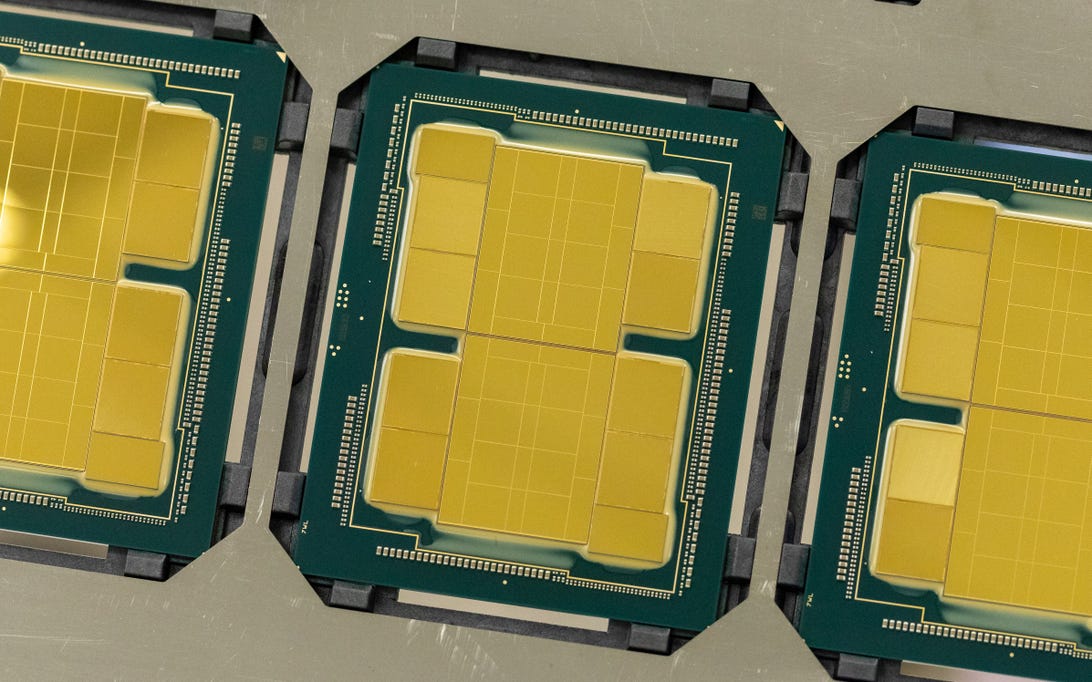
The retail on a whole spool of Sapphire Rapids chiplets must be pretty dang expensive... Probably has a few hundred chiplets on one spool.Really like the photo of the SPR chiplets on a spool.View attachment 53047
CNET posted a pretty cool article where they toured Intel's Arizona fab and they nabbed a few photos of Intel's future products, including Meteorlake:
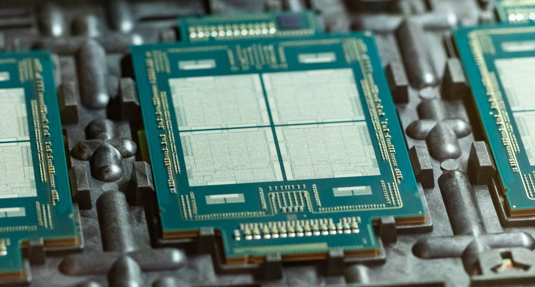
Anyone care to take a guess about the 4th chiplet for MTL?
Anyone care to take a guess about the 4th chiplet for MTL?
From the article, those are not real Meteor chips but samples for testing the bonding process. It's possible that the shapes are legit but it's not a given.
dullard
Elite Member
Visual Processing Unit, similar to Apple's M1 Neural Engine?Anyone care to take a guess about the 4th chiplet for MTL?
Intel's next-gen Meteor Lake will have integrated VPU accelerator
Intel's new Meteor Lake CPU architecture is getting a Neural Engine just like Apple uses in its new iPhone, for desktop + laptop.
 www.tweaktown.com
From the article, those are not real Meteor chips but samples for testing the bonding process. It's possible that the shapes are legit but it's not a given.
The shapes are indeed legit.
ashFTW
Senior member
Please see my explanation of the “HBM gap”. I’m pretty sure that’s the answer.Forgive me if I'm wrong here, since I don't know much about memory chips, but aren't the HBM connections central to the chip? Meaning that the gaps have to be wide?
https://en.wikipedia.org/wiki/High_...301-DSC10363_-_ZS-retouched_(29514443756).jpg
Discussion - Intel current and future Lakes & Rapids thread
Page 570 - Seeking answers? Join the AnandTech community: where nearly half-a-million members share solutions and discuss the latest tech.
forums.anandtech.com
Please see my explanation of the “HBM gap”. I’m pretty sure that’s the answer.
Discussion - Intel current and future Lakes & Rapids thread
Page 570 - Seeking answers? Join the AnandTech community: where nearly half-a-million members share solutions and discuss the latest tech.forums.anandtech.com
No, there isn't a second die that supports HBM.
ashFTW
Senior member
Based on what? There is clear evidence it that photo. You have a better explanation for 2 EMIB chiplet patters there with a big gap?No, there isn't a second die that supports HBM.
Last edited:
Based on what? There is clear evidence it that photo. You have a better explanation for 2 EMIB chiplet patters there with a big gap?
Well first of all, you do indeed need "pinout" for both the PHY and HBM, which explains why there are two. And the signal entering the HBM die from the middle is a perfectly adequate explanation.
Pick One. Arrow Lake is mobile only, or Meteor Lake is. Not both I don’t claim to have amazing sources, but hint: Intel is on a slightly-less-than-yearly cadence with desktop. Intel is currently following a tick tock with desktop/mobile. Big changes are mobile first.That is the rub. The same tweet thread that claims Meteor Lake is mobile only claims that Meteor Lake doesn't have a socket change. Those are highly unlikely to both be true.
Really like the photo of the SPR chiplets on a spool.View attachment 53047
Really? I never go out of my way to defend Intel, but that particular gossip piece has less relevance than me saying @maddie has poor taste in basically everything, details at 11!Who is the audience for this article? I assume the technologically ignorant.
This says it all.
"Intel has lagged TSMC and Samsung overall, but it's ahead with an increasingly important technology: chip packaging that lets Intel make a single processor out of multiple chip elements, variously called tiles, chiplets or dies."
EDIT: @maddie my comment is 100% nothing to do with you. I felt bad after posting it. What I meant to say was that any article claiming to have intimate details is flawed.
Given that MTL is almost 3 years out, I would hope…From the article, those are not real Meteor chips but samples for testing the bonding process. It's possible that the shapes are legit but it's not a given.
Indeed. I want to replace my butter with it.The shapes are indeed legit.
The shapes are indeed legit.
Problem with that is that the Big Die in the center is too big to be just the CPU or the GPU. It almost has to be both, and Intel's been saying that they were splitting them.
It looks like the UP4 package but a bit bigger.
ashFTW
Senior member
I disagree. We have seen only one EMIB chiplet at the edge in all the previous Intel implementations (e.g. See Ponte Vecchio). SPR will come with different chiplet sizes; Intel says UPTO ~400mm2 Per chiplet. SPR with HBM will likely come with two different SPR tile sizes as well, or at least it’s planned as a “backup” based on what AMD does. It could also just be for Aurora. Clearly it has been planned that way. We can agree to disagree and wait for Q1/Q2 next year.Well first of all, you do indeed need "pinout" for both the PHY and HBM, which explains why there are two. And the signal entering the HBM die from the middle is a perfectly adequate explanation.
Problem with that is that the Big Die in the center is too big to be just the CPU or the GPU. It almost has to be both, and Intel's been saying that they were splitting them.
It looks like the UP4 package but a bit bigger.
It's neither. That's the SoC die.
dullard
Elite Member
If that is the SoC in the middle, then it is a massive SoC.It's neither. That's the SoC die.
I very quickly measured the photo. Note: take these estimated sizes with a huge grain of salt, as I didn't bother with precise corrections due to oblique camera angles. The sizes are in the image below. I'm going to guess:
1) VPU?
2) SOC. The crudely estimated shape/size is roughly the same as Alder Lake's SOC, which would make sense if it is still on Intel 7. It probably doesn't change much.
3) CPU. This is a bit smaller in both directions than Alder Lake. Adding more E-cores roughly balances the density gain from Intel 4.
4) GPU. This is a bit more narrow and a bit longer than Alder Lake. Here is where I'm more skeptical of my chip assignments, since the area seems a bit too small in the photo, given additional GPU execution units. It would make sense though if this chip was produced at TSMC on a node smaller than Intel 7.

If that is the SoC in the middle, then it is a massive SoC.
I very quickly measured the photo. Note: take these estimated sizes with a huge grain of salt, as I didn't bother with precise corrections due to oblique camera angles. The sizes are in the image below. I'm going to guess:
1) VPU?
2) SOC. The crudely estimated shape/size is roughly the same as Alder Lake's SOC, which would make sense if it is still on Intel 7. It probably doesn't change much.
3) CPU. This is a bit smaller in both directions than Alder Lake. Adding more E-cores roughly balances the density gain from Intel 4.
4) GPU. This is a bit more narrow and a bit longer than Alder Lake. Here is where I'm more skeptical of my chip assignments, since the area seems a bit too small in the photo, given additional GPU execution units. It would make sense though if this chip was produced at TSMC on a node smaller than Intel 7.
View attachment 53074
The larger die seems to be the GPU tile.
locuza calculated the die sizes here:

The larger die seems to be the GPU tile.
locuza calculated the die sizes here:
View attachment 53075
It's the SoC die, not the GPU. That's the narrow one. And the 4th one isn't VPU either.
dullard
Elite Member
Thanks for the link, I had not seen those measurements.The larger die seems to be the GPU tile.
locuza calculated the die sizes here:
The difference is that link assumes a 2P+ 8E CPU. I assumed an 8P + 32E CPU. So, without knowing, we assigned a massively different size to the CPU chip.
dullard
Elite Member
The VPU is certainly just a guess based on one rumor that could be false. But why do you think the SoC chip more than doubles in size from Alder Lake to Meteor Lake?It's the SoC die, not the GPU. That's the narrow one. And the 4th one isn't VPU either.
The VPU is certainly just a guess based on one rumor that could be false. But why do you think the SoC chip more than doubles in size from Alder Lake to Meteor Lake?
Chipset features, VPU?, media?, SoC cores, worse process vs CPU/GPU dies, overhead from disaggregation, etc.
Also, that's definitely 2+8.
Last edited:
Why do you ignore the 6 core i7 desktop chips (i7 970 and i7 980) that Intel sold in 2010 and 2011 when AMD wasn't much of competition? These aren't even the Extreme Edition chips.
Intel only had those to compete with Thuban (6-core Phenom II). Once it became clear that an "8-core" Bulldozer wasn't really offering 8C levels of performance (or barely even 4C levels in some cases) Intel relegated anything with more than four cores to HEDT. Really those just prove the point even better and demonstrate how much Intel was willing to stagnate the market during that time.
TRENDING THREADS
-
 Discussion Zen 5 Speculation (EPYC Turin and Strix Point/Granite Ridge - Ryzen 9000)
- Started by DisEnchantment
- Replies: 25K
-
Discussion Intel Meteor, Arrow, Lunar & Panther Lakes + WCL Discussion Threads
- Started by Tigerick
- Replies: 25K
-
 Discussion Intel current and future Lakes & Rapids thread
- Started by TheF34RChannel
- Replies: 24K
-

-
