coercitiv
Diamond Member
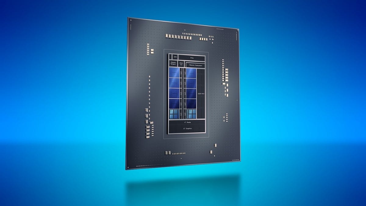
According to Intel themselves it should be the start, they briefed the press on MTL using 3 dies: compute die, SOC-LP die and GPU die.I just don't know if Meteor Lake is the start of it.

According to Intel themselves it should be the start, they briefed the press on MTL using 3 dies: compute die, SOC-LP die and GPU die.I just don't know if Meteor Lake is the start of it.
According to Intel themselves it should be the start, they briefed the press on MTL using 3 dies: compute die, SOC-LP die and GPU die.
I hope not, that woupd artificially cap their potential. I do beliece more IGP options are good to have. More options period.
Competition is good, but two companies isn't competition--it is a duopoly. And Intel had 8 cores well before Ryzen. It was just in their Extreme Edition desktops. https://ark.intel.com/content/www/u...extreme-edition-20m-cache-up-to-3-50-ghz.htmlIsn't competition grand? Intel would probably still be on hex cores if it wasn't for Ryzen. Instead it looks like we'll be getting some great new hybrid CPU that crushes it in the benchmarks if nothing else.
Isn't competition grand? Intel would probably still be on hex cores if it wasn't for Ryzen. Instead it looks like we'll be getting some great new hybrid CPU that crushes it in the benchmarks if nothing else.
This was already addressed with Lakefield, the scheduler identifies foreground tasks and attempts to schedule them on P cores. Critical workloads don't start on the E cores unless all P cores are already busy doing other critical work.Like a time critical workload starting on the E core
This was already addressed with Lakefield, the scheduler identifies foreground tasks and attempts to schedule them on P cores. Critical workloads don't start on the E cores unless all P cores are already busy doing other critical work.
Then why did we need new version of Windows?
I arrive at 532.7 for Gracemont
Small cores scores about 400 pts@3.7GHz in CB R20 and 1040pts in CB R23.
Link?
All workloads start on P cores unless (A) it is a background task as already identified in old or new software, (B) new software identifies it as an E core task, or (C) all P cores are busy with higher priority tasks that are actively doing work.Like a time critical workload starting on the E core then a context switch and core to core bandwidth consumption as the Intel Thread Director realizes it needs more power and shifts it to a P core. That will consume precious cycles and add latency.
Item (C) is why Windows 11 was needed. In the past, threads were scheduled using rules-of-thumb. That is, they were scheduled without knowing if the cores or workloads were busy or not and without knowing if the cores were hot (and needing to be thermally throttled back) or cold (and could be ramped up to turbo speeds).Then why did we need new version of Windows?
On my previous post.
So at 4000 mHz frequency, does that work out to 50/(4*10^9/s) = 12.5 ns latency?Hm, 8000mhz with CL50 latency.
I don't see it? The link I mean.
Despite an efficient design, the Alder Lake E-core still packs a punch. At the same frequency, it offers the same general purpose integer performance per clock as Skylake at a fraction of the power.
Alder Lake introduces a new client SoC architecture that scales from powerful desktops to…
Author: Marcus Yam, Technology Evangelist at Intelmedium.com
FTR RKL does 453.7 pts/3.7GHz in CB R20, your 532 pts /3.7Ghz is 10% better than a Zen 3 and close to what is expected from ADL P cores .
DDR5 is pretty crazy. Just recently that was GPU memory. I can't help but wonder what DDR5 could mean for APUs. If DDR5 for desktop is fast enough, is there any reason that a motherboard couldn't have two sockets; one for CPU and one for GPU? Imagine an upgradeable GPU that drops into your motherboard? It has to happen. Tell me it's stupid and I'll say YOUR STUPID.
DDR5 is pretty crazy. Just recently that was GPU memory. I can't help but wonder what DDR5 could mean for APUs. If DDR5 for desktop is fast enough, is there any reason that a motherboard couldn't have two sockets; one for CPU and one for GPU? Imagine an upgradeable GPU that drops into your motherboard? It has to happen. Tell me it's stupid and I'll say YOUR STUPID.
DDR5 is pretty crazy. Just recently that was GPU memory. I can't help but wonder what DDR5 could mean for APUs. If DDR5 for desktop is fast enough, is there any reason that a motherboard couldn't have two sockets; one for CPU and one for GPU? Imagine an upgradeable GPU that drops into your motherboard? It has to happen. Tell me it's stupid and I'll say YOUR STUPID.