At least 5 users here state it daily that Willow is a 8% increase over ICL and use that as a seemingly unquestionable proof that Zen 3 will have lower IPC than the current intel CPU when it comes out.. . . hmm. Didn't Intel already hint at that? Something about Sunny Cove and Golden Cove being the uarch steps that brought IPC gains while Willow Cove was more focused on restructing cache?
-
We’re currently investigating an issue related to the forum theme and styling that is impacting page layout and visual formatting. The problem has been identified, and we are actively working on a resolution. There is no impact to user data or functionality, this is strictly a front-end display issue. We’ll post an update once the fix has been deployed. Thanks for your patience while we get this sorted.
You are using an out of date browser. It may not display this or other websites correctly.
You should upgrade or use an alternative browser.
You should upgrade or use an alternative browser.
Discussion Intel current and future Lakes & Rapids thread
Page 179 - Seeking answers? Join the AnandTech community: where nearly half-a-million members share solutions and discuss the latest tech.
IntelUser2000
Elite Member
Effectively same IPC as ICL-U. Use Linux scores like this: https://browser.geekbench.com/v5/cpu/941452.gb5 for comparison.
Also, GB5 on Linux reports ST Turbo as base frequency, the .gb5 shows the true base of 1.8GHz. This is probably 15W config.
Do I need to remind you people of the futility of comparing using user submitted benchmarks?
There's a XPS 13 Icelake score that gets 553/1560 points using the same OS version but its running at 2600MHz. According to that, one 1065G7 is 76% faster per clock than the other 1065G7 in the same system!
Dell Inc. XPS 13 7390 2-in-1 - Geekbench
Benchmark results for a Dell Inc. XPS 13 7390 2-in-1 with an Intel Core i7-1065G7 processor.
 browser.geekbench.com
Dell Inc. XPS 13 7390 2-in-1 - Geekbench
Benchmark results for a Dell Inc. XPS 13 7390 2-in-1 with an Intel Core i7-1065G7 processor.
browser.geekbench.com
Same compilers too. And they are submitted 3 within days of each other. Intel does lot of Linux work and might be doing testing based on it.
I'm talking about bugs, bios and software optimizations, misconfigurations, different TDP etc, everything is unknown. The MT score of this entry is a good example, there is no explanation why this sample scores 1000 points higher.
Linux is faster for Icelake in ST but slower in MT according to the results. It's same with Tigerlake.
We're not seeing Tigerlake with the latest Ubuntu 19 version. Tigerlake is on Ubuntu 16. The top 1065G7 results are all using Ubuntu 19.
And by the way, Geekbench has absolutely no way to sort. Horrible.
Last edited:
DrMrLordX
Lifer
Comparing across different OSes is never a good idea with Geekbench. The results get weird.
Just wanted to point out that that's less of an issue with GB5. GB4 used different compilers (I guess?) between OSes so it ran faster in Linux.
IntelUser2000
Elite Member
All Cometlake dies.
-U: 2/4/6
-H: 4/6/8
-S: 6/8/10
Different Linux versions also have different performance.
-U: 2/4/6
-H: 4/6/8
-S: 6/8/10
Just wanted to point out that that's less of an issue with GB5. GB4 used different compilers (I guess?) between OSes so it ran faster in Linux.
Different Linux versions also have different performance.
Icelake die size = 122mm^2 (wikichip)
Tiger lake die size = 155.0413 mm^2
L2 512KB →1.25MB
L3 2MB →3MB
GPU 64EU →96EU
Gideon
Platinum Member
Tiger lake die size = 155.0413 mm^2
Meanwhile Francois Piednoel is arguing that Renoir is totally doomed to make any profits because its .... about 150 mm^2 😀
coercitiv
Diamond Member
Nvm, I just read the post above yours, the irony is better illustrated there.Meanwhile Francois Piednoel is arguing that Renoir is totally doomed to make any profits because its .... about 150 mm^2 😀
Meanwhile Francois Piednoel is arguing that Renoir is totally doomed to make any profits because its .... about 150 mm^2 😀
Geez, Intel 10nm will never be 'fully blasting'. And my google skills are failing me, what is the size of an Intel 8 core laptop CPU?
Totally being pedantic here, but the total number of new dies for Comet Lake will only be between 2 and 4.All Cometlake dies.
-U: 2/4/6
-H: 4/6/8
-S: 6/8/10
For platforms you have the following:
CML-Y 2/4C
CML-U v1 (LP3) 2/4/6C
CML-S 2/4/6/8/10C
CML-H 8/10C (possibly lower core count as well)
CML-U v2 (LP4x) 2/4/6C
Intel decided to go with the Comet Lake Y name in their public announcements of AML-Y 4+2, which is actually built using the WHL-U 4+2 V0 die in conjunction with the SPT-LP PCH.
CML-U v1 launched as 6 SKUs, only one of which requires the new A0 6+2 die. The others can all be made using the WHL-U 4+2 V0 die, however they should all be paired with the 400 Series CMP-LP (a.k.a. ICP-LP) PCH. In fact, it appears that the Core i7-10510U, the highest clocked 4-core model, can only be built from the older V0 die. Obviously the V0 die does not have LPDDR4X support, and if A0 does then it has yet to be enabled for any available SKU.
The S and H platforms generally share dies. CML-S will clearly require a new 10+2 die, and Intel has indicated that the majority of the product stack will be built from 6+2 and 10+2 dies in LGA1200 packages. The cynical side of me thinks the original CFL-H/S 6+2 U0 die may make another appearance here, but being stepping 10 it is due for a refresh for security patches if nothing else. The PCH is a separate package for the H/S platforms, and H CPUs are sticking with BGA1440, so all of the lower core count CML-H SKUs can just be renamed Coffee Lake / Coffee Lake Refresh chips.
CML-U v2 should finally bring LPDDR4x support, and the A0 die may well be capable of that already, especially seeing as how it carries the entirely new 166 model number. However, Intel may do a second stepping of 6+2 or a proper CML-U 4+2 v2 die to replace the current WHL-U 4+2 die.
edit: clarify CML-H/S packaging situation.
Last edited:
Nothingness
Diamond Member
For ST only the libc/libm should matter (and it does for some of the tests), that indirectly depends on the Linux distro/version. Just nitpicking 🙂Different Linux versions also have different performance.
Icelake die size = 122mm^2 (wikichip)
Tiger lake die size = 155.0413 mm^2
Apparently the die size of Tigerlake is something between 132-145 mm². PCIe4, LPDDR5, slightly bigger CPU cores, possibly 25% bigger GPU and bigger L2 and L3 cache size.
beginner99
Diamond Member
Meanwhile Francois Piednoel is arguing that Renoir is totally doomed to make any profits because its .... about 150 mm^2 😀
But why with tiger lake this huge? It's only 4 cores? Xe graphics seem to be pretty bad performance/size wise.
thesmokingman
Platinum Member
Meanwhile Francois Piednoel is arguing that Renoir is totally doomed to make any profits because its .... about 150 mm^2 😀
Nah, he ain't biased. As if AMD doesn't know wtf they are doing up to this point.
But why with tiger lake this huge? It's only 4 cores? Xe graphics seem to be pretty bad performance/size wise.
Tigerlake isn't huge, actually it's surprisingly small compared to Icelake with these added features. The Xe architecture seems to get a much improved area efficiency. Renoir has a smaller GPU and fewer features like no PCIe4, no LPDDR5 controller, no AVX512, smaller CPU cache for each core+ lower IPC and nevertheless it's slightly bigger.
beginner99
Diamond Member
Renoir has a smaller GPU and fewer features like no PCIe4, no LPDDR5 controller, no AVX512, smaller CPU cache for each core+ lower IPC and nevertheless it's slightly bigger.
But renoir has double the CPU cores.
IntelUser2000
Elite Member
For ST only the libc/libm should matter (and it does for some of the tests), that indirectly depends on the Linux distro/version. Just nitpicking 🙂
I looked at about 10 results. The 19 version is clearly faster than the other Linux versions in Geekbench.
But Linux distros are slower than Windows for multi-threading despite having better performance for single thread.
There's too many variables to reliably conclude which CPU is 5% faster.
But renoir has double the CPU cores.
The two are about the same die size.
AMD put more on CPU, Intel more on GPU.
I'm kinda surprised at the die size of Renoir. I expected it to be smaller if its 8 CUs. Maybe it shrunk 30% like with Vega VII.
Gideon
Platinum Member
Ice-Lake is 122mm^2. The 50% extra EUs are probably the bulk of the size-increase and the next one is the added cache. AVX-512 also takes up considerable space (compare server Skylake to desktop) though that's already included in Ice-Lake.But why with tiger lake this huge? It's only 4 cores? Xe graphics seem to be pretty bad performance/size wise.
Come on now. Saying "Renoir is bigger" and listing all the differences you can find, expect the the "minor" one that it has twice the cores, isn't a fair comparison.Renoir has a smaller GPU and fewer features like no PCIe4, no LPDDR5 controller, no AVX512, smaller CPU cache for each core+ lower IPC and nevertheless it's slightly bigger.
Besides, Ian Cutress estimated Renoir at 148mm^2 (~150mm2). The upper poster estimated Tiger Lake is 155mm^2. Overalll the die sizes are in flux enough to say that they are about the same. Especialy when taking into account what some have claimed previously, that Intel's 10nm is denser than TSMC 7nm.
As for PCIe4 - AMD's IF is built upon that and AMD uses it internally in their chips. I'm pretty sure Renoir has support for it internally and we'll have it in desktop versions. They probably cut it on laptops for power reasons. LPDDR5 controller shouldn't add much space compared to LPDDR4X.
All in all, I do agree that it's impressive that they managed to cram both the extra cache and EUs in ~150mm^2.
Last edited:
IntelUser2000
Elite Member
Maybe Renoir is 11CU but they are not using it on mobile, yet.
From the AT article:
however AMD has reasons for that decrease and emphasized that due to the process node they can get 8 CUs to perform better than 11 CUs.
RetroZombie
Senior member
And also integrates the south bridge.But renoir has double the CPU cores.
Come on now. Saying "Renoir is bigger" and listing all the differences you can find, expect the the "minor" one that it has twice the cores, isn't a fair comparison.
Besides, Ian Cutress estimated Renoir at 148mm^2 (~150mm2). The upper poster estimated Tiger Lake is 155mm^2.
I told Renoir is slightly bigger which I'm sure is correct! Are you crazy or what? Furthermore the upper poster source removed his posting and corrected his calculation and now says 145 mm², so you are not well informed. However the die size based on the Tigerlake wafer appears to be smaller towards 140mm² or below. Come on now.
Based on this Tiger Lake wafer, there are 23 dies across and almost 28 dies vertically, meaning that 4C+96EU Tiger Lake has a ~140mm^2 die.
Assuming Intel is better at dicing up the wafer, and only has a 0.15mm scribe lane, and also matching it up more exactly to the partial wafers out to the edges, I can get the chips to 12.7mm x 10.4mm for 132 mm^2
If we take 1 unit = 10.82 mm Then : Tiger lake width = 10.82 mm Tiger lake height = 1.24 * 10.82 = 13.4168 mm Tiger lake die size = 145.17 mm
Nothingness
Diamond Member
Ubuntu 19 uses glibc 2.29I looked at about 10 results. The 19 version is clearly faster than the other Linux versions in Geekbench.
That's what I had in mind. Might be a reason... or not.Optimized generic exp, exp2, log, log2, pow, sinf, cosf, sincosf and tanf.
Yes definitely. One should pick dozens of results to make a comparison within that range.There's too many variables to reliably conclude which CPU is 5% faster.
Tigerlake isn't huge, actually it's surprisingly small compared to Icelake with these added features. The Xe architecture seems to get a much improved area efficiency. Renoir has a smaller GPU and fewer features like no PCIe4, no LPDDR5 controller, no AVX512, smaller CPU cache for each core+ lower IPC and nevertheless it's slightly bigger.
You might want to read you post again. What is it we dont understand?
"nevertheless it's slightly bigger."
Its nonsense. Or you simply forgot 4 cores and some io in your confirmation bias ...
and nevertheless it's slightly bigger.
Errr... a Zen 2 core is 3.64 mm2 including L2 (per wikichip)... Sunny Cove is 6.91.Willow has to be bigger than that.
IntelUser2000
Elite Member
I told Renoir is slightly bigger which I'm sure is correct! Are you crazy or what? Furthermore the upper poster source removed his posting and corrected his calculation and now says 145 mm², so you are not well informed. However the die size based on the Tigerlake wafer appears to be smaller towards 140mm² or below. Come on now.
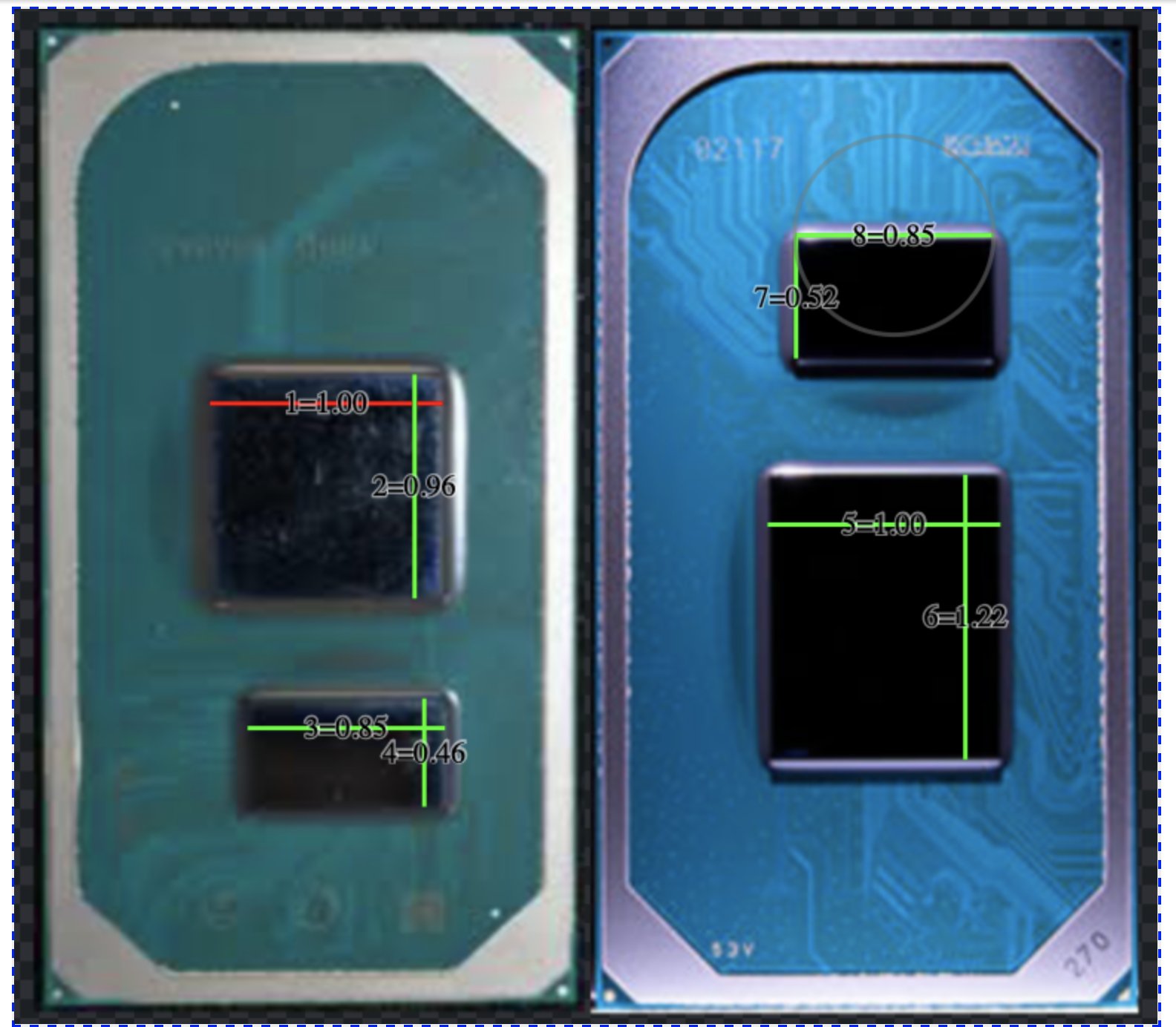
I got 146mm2, and I used paint, and assumed the PCH is same at 53mm2.
This estimate also supports my theory that Tigerlake just became longer, and the long:short ratio went from 1.05 in ICL to 1.25, also getting us the 145mm2 figure.
Ian got his 150mm2 estimate of Renoir by basically eyeballing.
Exact measurements can often be more off(as the delete post used) as it does not account for the possible errors introduced by camera angles and the raised die section messing up things.
I told Renoir is slightly bigger which I'm sure is correct!
This is AT nerd form of a dick measuring contest. However they are not measuring the size of their own, but Intel/AMDs. With errors being plus or minus 2-3mm2 easily, we can also conclude they are the same.
TRENDING THREADS
-
 Discussion Zen 5 Speculation (EPYC Turin and Strix Point/Granite Ridge - Ryzen 9000)
- Started by DisEnchantment
- Replies: 25K
-
Discussion Intel Meteor, Arrow, Lunar & Panther Lakes + WCL Discussion Threads
- Started by Tigerick
- Replies: 25K
-
 Discussion Intel current and future Lakes & Rapids thread
- Started by TheF34RChannel
- Replies: 24K
-

-
