LPDDR4 isn't supposed to be in the initial CML-U chips?
The first wave of Comet Lake-U is just renamed, it's a stepping 12 of Whiskey Lake says Geekbench. No chance for LPDDR4.

LPDDR4 isn't supposed to be in the initial CML-U chips?
The new fabrication process enables chip designers to reuse 7LPP IP on ICs designed for 5LPE while enjoying all benefits the latter provides. When compared to 7LPP, the new technology has an up to 25% higher ‘logic efficiency’, it also enables chip developers to reduce power consumption of their designs by 20% or improve their performance by 10%.
In a related news:
Samsung’s 5nm EUV Technology Gets Closer: Tools by Cadence & Synopsys Certified
At this point if I were an Intel CEO I would start producing Ice Lake CPUs using Samsung's foundries.
Samsung's 5nm is nowhere near TSMC 5nm or Intel's 7nm in terms of density.
I'm sure they could if they really wanted to, I mean heck there are existing 6C chips with 9MB L3. In fact the very laptop I am typing this on is an 8750H with 9MB L3.And 7MB of L3 make very little sense as well. For example 6C dies have 6 partitions of 2MB of L3 cache. Can't really reduce that to 7MB?
I'm sure they could if they really wanted to, I mean heck there are existing 6C chips with 9MB L3. In fact the very laptop I am typing this on is an 8750H with 9MB L3.
Can it compete with Intel 10nm in density? And, unlike Intel 10nm, can it function?
Samsung's 5nm is nowhere near TSMC 5nm or Intel's 7nm in terms of density. Samsung's "3nm" is competing against those nodes and it won't be ready until 2022.
And by the way TSMC 7nm doesn't look impressive based on Zen2 , it only clocks to 4200-4300 Mhz typically with a pretty high Vcore demand.....only marginally better than 12nm.
Guessing more Rocket, which uses Icelake's platform.
The first wave of Comet Lake-U is just renamed, it's a stepping 12 of Whiskey Lake says Geekbench. No chance for LPDDR4.
It seems like Samsung's 5nm EUV is comparable to TSMC's 7nm+ in terms of density, so should be little more dense than Intel's 10nm. We haven't even got a first look at Samsung's 7nm which first product based on it isn't due until early next year so hard to say how it is going to perform.
"Comet Lake = renamed Whiskey Lake" is a process limitation. I mean, isn't everything 14nm just renamed Skylake?
Whiskey Lake itself was just Kaby Lake-R, but it includes a handful of Spectre/Meltdown mitigations in hardware that apparently don't give away as much performance as the software mitigations.
Not that consumers really felt Spectre/Meltdown, anyways. The "meh" cooling of Whiskey Lake in dreadful 15 W chassis laptops probably had a larger effect.
Yeah it's kinda funny that Intel having spent so much time optimizing 14nm will sort of make it harder to move to 10nm and 7nm as they have truly optimized the crap out of that 14nm process. It will take quite some time and tuning to get a future process to that level...
Even Skylake wasnt that great of a clocker, it wasnt until Kaby Lake that they really got the clocks up.
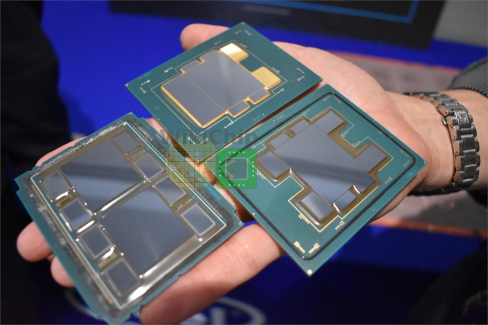
It looks like what AMD has already done in Ryzen2/Rome.Intel announces new packaging stuffs at SemiCon West. Co-EMIB, ODI and MDIO
Article from the EETImes, WikiChip, ServeTheHome and Venture Beat
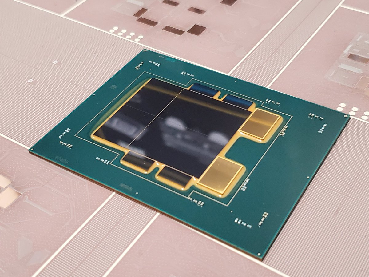
The chips they showed looked really cool and are based on 10nm.
Skylake 4 core + iGPU has ~1.7 billion transistors? Bristol Ridge had 3 billion or so? Ryzen without iGPU has 4.9 billion?
Don't think there is Rocket suitable for Macbook or Macbook air on leaked roadmap.
The chips they showed looked really cool and are based on 10nm.
It looks like what AMD has already done in Ryzen2/Rome.
I assume all 10nm since that is what David said. If some were 14nm I am sure he would have said so...Not all may be 10nm. They want to deliver two near full reticle sized Cascade Lake in a single package.
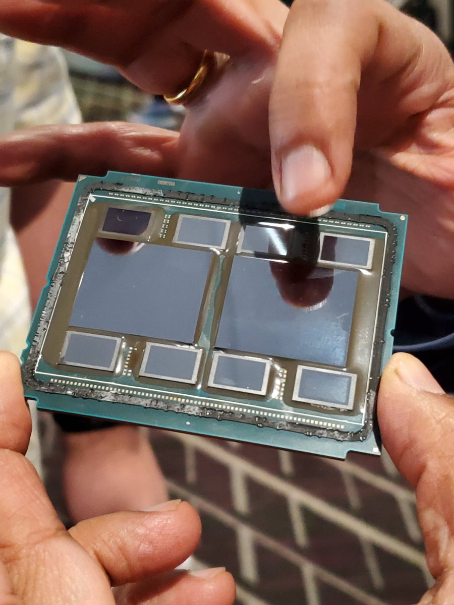
Could also be that rumored Icelake MCM CPU with HBM2The package above with what seems like two very large dies plus 8 small ones could be Cooper Lake AP, using two Cascade Lake SP dies.
Cooper Lake AP with 56 cores + 8 stack HBM2 memory for 1TB/s bandwidth?
I assume all 10nm since that is what David said. If some were 14nm I am sure he would have said so...
The Cascade Lake-AP line is bit of a disappointment now, but with HBM2 stacks enabling much increased memory bandwidth, and possibly using EMIB could allow it to carve a niche.