Discussion Intel current and future Lakes & Rapids thread

Page 27 - Seeking answers? Join the AnandTech community: where nearly half-a-million members share solutions and discuss the latest tech.

jpiniero

Lifer
Oct 1, 2010
14,510
5,159
136

Isn't that what PAO is supposed to be?

Process = Cannonlake
Architecture = Icelake
Optimization = Tigerlake

So now that Cannonlake is all but dead; and they can't do 10 nm server products without EMIB because of the awful yield... sooo it kind of makes sense to just skip Icelake Server too and just go to Tigerlake since it was built with 10++ in mind and presumably EMIB too.

Ice Lake Refresh refers to a refresh of the platform to include an Ice Lake-based processor family.

I dunno... seems to fit perfectly to go straight to Tigerlake since they need EMIB.
 

Ajay

Lifer
Jan 8, 2001
15,332
7,792
136
Isn't that what PAO is supposed to be?

Process = Cannonlake
Architecture = Icelake
Optimization = Tigerlake

So now that Cannonlake is all but dead; and they can't do 10 nm server products without EMIB because of the awful yield... sooo it kind of makes sense to just skip Icelake Server too and just go to Tigerlake since it was built with 10++ in mind and presumably EMIB too.


I dunno... seems to fit perfectly to go straight to Tigerlake since they need EMIB.

EMIB for Tigerlake client?? Things are effed up, so what Intel's actual roadmap is now is questionable. Rumors indicated that 10nm+ is having issues, which sucks for Intel and users alike. I would prefer to find more info though - at least a Digitimes article so we have a better idea of what is what in Intel's coming product stack.
 

Dayman1225

Golden Member
Aug 14, 2017
1,152
973
146
https://software.intel.com/sites/de...tion-set-extensions-programming-reference.pdf

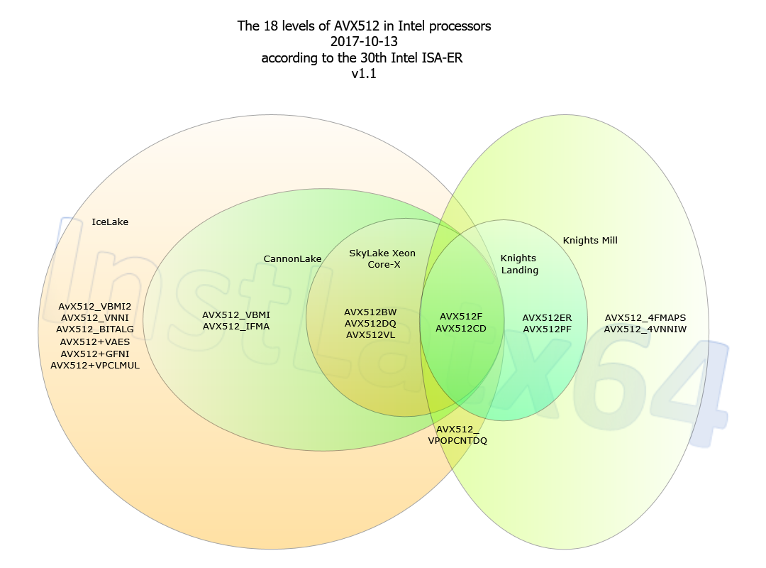
Updated Instruction Set from Intel, includes Icelake, Cannonlake and Goldmont Plus

DL9X76IXkAMtyxk.jpg

DL9YDM_XUAAzqYI.jpg
DL9YImBXkAAE795.jpg
 

Bouowmx

Golden Member
Nov 13, 2016
1,138
550
146
Investing the density increase of 10 nm to add AVX-512 to everything, even a Cannon Lake laptop. Except Atom. Unless the document did not bother to differentiate client and server.
 

Dayman1225

Golden Member
Aug 14, 2017
1,152
973
146
AFAIK Cannonlake is now only mobile, I suppose the CNL 2+2 70mm^2~ die size makes a little more sense now? Though AVX512 on what is only Y/U parts is a bit weird, no?
 

Bouowmx

Golden Member
Nov 13, 2016
1,138
550
146
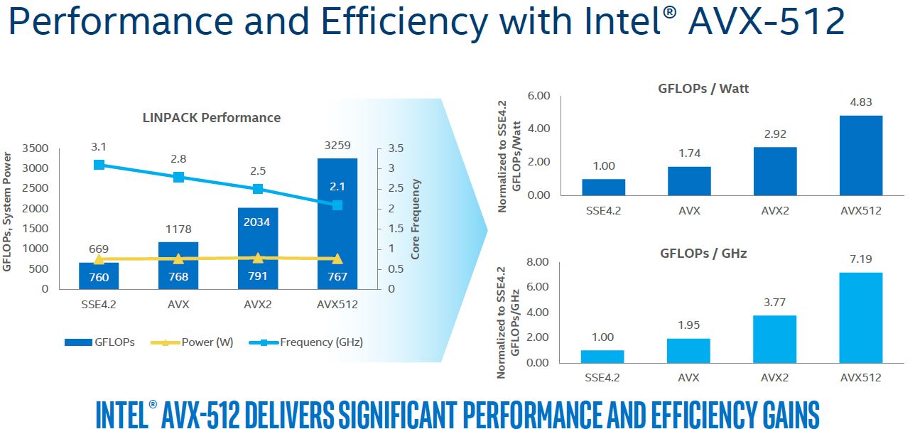
Theoretically, more FLOPS can be done with AVX-512, without increase in power from AVX2, if AVX-512 is offset in frequency. If you happen to use an app that supports AVX-512, on a laptop, more productivity on battery? Quite a stretch.
Intel-Skylake-SP-Microarchitecture-AVX-512-Performance.jpg
 

JoeRambo

Golden Member
Jun 13, 2013
1,814
2,105
136
AFAIK Cannonlake is now only mobile, I suppose the CNL 2+2 70mm^2~ die size makes a little more sense now? Though AVX512 on what is only Y/U parts is a bit weird, no?

AVX512 instruction support does not mean Intel has to include 512bit wide vector units, as shown by AMD and AVX2/FMA support without actual 256bit units. But that is speculation of course.
Still, for mobile it is inefficient to even include the massive register file required for AVX512F support as that bloats things up big time.
 
  • Like
Reactions: Dayman1225

inf64

Diamond Member
Mar 11, 2011
3,685
3,957
136
AVX512 will just bloat these chips up big time. Average Joe doesn't care about that if there is no effect on apps he runs every day. Better invest the die space in something that matters, like iGPU or cache, better int performance, higher clock.
 
  • Like
Reactions: Drazick and NTMBK

JoeRambo

Golden Member
Jun 13, 2013
1,814
2,105
136
I've noticed in the table above, that Ice Lake will have Fast Short REP MOV support. That could actually have a larger impact in crazy memcpy land we have now. Instead of crazy optimizations, where sizes, aligments, AVX256/512 instruction madness, future memcpy's could run each case with REP MOVs instead. Great real world optimization.
 
  • Like
Reactions: Arachnotronic

Ajay

Lifer
Jan 8, 2001
15,332
7,792
136
AVX512 will just bloat these chips up big time. Average Joe doesn't care about that if there is no effect on apps he runs every day. Better invest the die space in something that matters, like iGPU or cache, better int performance, higher clock.

I don't think AVX512 will be found in client cores anytime soon - well, I hope not. I would really be more of a marketing gimmick, IMHO, given standard client workloads.
 
Mar 10, 2006
11,715
2,012
126
I don't think AVX512 will be found in client cores anytime soon - well, I hope not. I would really be more of a marketing gimmick, IMHO, given standard client workloads.

Looks like it's been added to CNL and beyond.
 

krumme

Diamond Member
Oct 9, 2009
5,952
1,585
136
Yeah, but it just doesn't make sense. IDK what Intel is thinking - other than creating a bogus marketing checkbox?
Naa. Perhaps its the old monopoly thinking. Avx512 entrenches your position. Its just the highly effective dual fp in ryzen just tears down that wall head on. Makes the avx512 looks like the Maginot line. Stoneage thinking.

I think the wide fpu exposes what is wrong in Intel. There is simply a lack of technology leadership connected to how the business environment is developing. Add Slow changing. Unflexible huge organization. We have seen this thousands times before. Textbook example.
 

NTMBK

Lifer
Nov 14, 2011
10,208
4,940
136
Looks like it's been added to CNL and beyond.

My guess is that they'll do it by splitting ops across the two AVX-256 ports, similar to how to the "first" AVX-512 FMA works in SKX. I doubt we'll see the second FMA turn up.

Gives you software compatibility, increased register space, and the improved instruction set (e.g. operation masking, scatter instruction) without blowing up the core size/power budget too much.
 
  • Like
Reactions: Arachnotronic

IntelUser2000

Elite Member
Oct 14, 2003
8,686
3,785
136
I think the wide fpu exposes what is wrong in Intel.

If they decide to add HBM stacks with EMIB-toting server chips, the extra FPU power would be entirely justified. The regular Xeon cores are too bandwidth limited to take advantage of even AVX-256 fully. Knights Landing does however, because of the MCDRAM's bandwidth.

Accelerators like media/GPU, FPGA, Deep Learning units are on the cards for near future Intel server chips. And its said Intel does plan to utilize HBM, which is a nice match.

Yeah, but it just doesn't make sense. IDK what Intel is thinking - other than creating a bogus marketing checkbox?

For client I think AVX2 would suffice for quite a while. There are rumors that they might go even larger than AVX-512 though. I think AVX-1024 would have been a nice addition to Knights Hill, as if they could boost clocks or cores by 20-25%, we'd have 8TFlop DP @ 200W which is quite nice. Unfortunately that doesn't seem to be the case.
 

Dayman1225

Golden Member
Aug 14, 2017
1,152
973
146
Media Alert: Intel CEO Brian Krzanich Will Kick Off CES 2018 with Pre-Show Keynote
https://newsroom.intel.com/news-rel...-krzanich-kick-off-ces-2018-pre-show-keynote/

> me implying possible announcements of products in thread title


I believe they also have an event just before SC17, might see some updates on Lake Crest/Knights Crest and some other products. I also hear there is a investors day in February(not 100% sure) maybe we'll see something like a 10nm yield graph like they did with 14nm, of just information on their 10nm/products in general.
 

jpiniero

Lifer
Oct 1, 2010
14,510
5,159
136
2020 is Sapphire Rapids. Maybe ;)

EMIB is a big enough change that doing that and an entirely redesigned CPU core seems much.
 

Bouowmx

Golden Member
Nov 13, 2016
1,138
550
146
That's not saying much, which is to say Ice Lake is to Tiger Lake as Sandy Bridge is to Ivy Bridge. Improved process and CPU/GPU architecture, some familiar grounds. I suppose the intended message is Ice Lake to Tiger Lake is not Skylake to Kaby Lake, which is no change in CPU architecture and overclock through improved process.
 
  • Like
Reactions: Dayman1225

Dayman1225

Golden Member
Aug 14, 2017
1,152
973
146
That's not saying much, which is to say Ice Lake is to Tiger Lake as Sandy Bridge is to Ivy Bridge. Improved process and CPU/GPU architecture, some familiar grounds. I suppose the intended message is Ice Lake to Tiger Lake is not Skylake to Kaby Lake, which is no change in CPU architecture and overclock through improved process.

To me this means Intel is starting to get back to its old self. It also makes me believe Intels 10nm product stack is one of their best planned out in the last few years. Allowing themselves more time for possible future process delays. Just better planning in general IMO
 

krumme

Diamond Member
Oct 9, 2009
5,952
1,585
136
To me this means Intel is starting to get back to its old self. It also makes me believe Intels 10nm product stack is one of their best planned out in the last few years. Allowing themselves more time for possible future process delays. Just better planning in general IMO
I tend to agree. Its realistic. Perhaps top management stopped praying to the holy Moores law and asked what is actually happening. We used to get some good ipc tick. Perhaps 1% doesnt sound like much but it adds up and the tock hits a wall to.
A classic example of a fantastic tick is core duo. It nearly redefined what you could do with a laptop and was so fast even a ssd x25 made sense in win 7.
The effect of a well planned tick can be big.
 
  • Like
Reactions: Dayman1225

NTMBK

Lifer
Nov 14, 2011
10,208
4,940
136
Hmm, how much would the physical register file actually grow to implement AVX-512? It has wider registers and more named registers, but the physical register file is already larger than logical register space (to allow register renaming for OoO). Presumably adding the mask vector registers will require special support, but would the 512-bit vectors actually grow the size at all? Especially considering that those 512-bit vectors are cracked into 256-bit halves to send to the separate 256-bit ports? I'm not overly familiar with the current structure of PRF in Skylake.