I agree with krumme. It's all marketing jargon. Now marketing is a necessity for companies. It's fine, until they start pulling this nonsense.
Huawei Kirin 970 achieves 55 mil tr/mm2 in a product form. Intel claims TSMC has a density of 50 mil tr/mm2. That is a fantastic achievement. With Intel if you want to see a real world example that meets that criteria you have to dig deep. Like in SRAMs, where with Skylake cores you see it taking a miniscule amount of space(indicating it isn't even being used en masse). They had to cut L3 in Skylake-SP as well. The only part of the core where their density advantage starts to show strength they have to cut it.
I'll tell you more examples of theoretical advantage not translating into actual products. They claimed with 14nm Airmont core, the density advantage over a 22nm Silvermont one was 2.8x. Despite that, they went from a ~105mm2 die on Bay Trail to ~85mm2 on Cherry Trail.
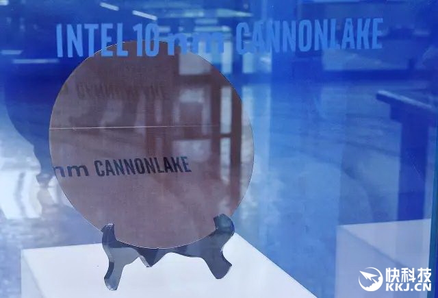
With 14nm Knights Landing, it has a die size greater than 650mm2. Intel said it has 8 billion transistors. The density then is ~12 mil tr/mm2, far short of 28 mil tr/mm2 they claim on that slide.
Now I can tell you why they might have to do this. Their cores are usually reserved for very high clocks, and in that case the densest transistors can't always be used. But considering how well Apple is doing, and even smaller companies like Huawei, its a far-fetched excuse.
So you can meet Intel's density claims if you end up designing a chip with 90% SRAMs(cache) by area, or slow, simple chips. Great.