In this case, Intel themselves decided to try and jump over a 40 m tall fence while carrying a backpack that weighs 5 tons. Every time they tried to jump and fell back after 3 cm, they kept reassuring everyone that everything is fine, we're currently flying, totally mid-air and we'll arrive on the other side at the planned date. Then a year after the planned date, they took a polaroid picture of themselves, named it cannon lake and threw it over the fence.There's never been a time where the whole industry hit a wall, so I see no reason to expect that in the future. If one company hits a wall their chances of recovery and catching up become more dim with each cycle because missing out on that juicy early depreciation really hits the bottom line. I expect either Intel or Samsung to fall out of the race before the end of the decade, then we'll see what happens when it is down to just two.
-
We’re currently investigating an issue related to the forum theme and styling that is impacting page layout and visual formatting. The problem has been identified, and we are actively working on a resolution. There is no impact to user data or functionality, this is strictly a front-end display issue. We’ll post an update once the fix has been deployed. Thanks for your patience while we get this sorted.
You are using an out of date browser. It may not display this or other websites correctly.
You should upgrade or use an alternative browser.
You should upgrade or use an alternative browser.
Discussion Intel current and future Lakes & Rapids thread
Page 582 - Seeking answers? Join the AnandTech community: where nearly half-a-million members share solutions and discuss the latest tech.
igor_kavinski
Lifer
Aha! So that's why they called it Cannon Lake! 😀In this case, Intel themselves decided to try and jump over a 40 m tall fence while carrying a backpack that weighs 5 tons. Every time they tried to jump and fell back after 3 cm, they kept reassuring everyone that everything is fine, we're currently flying, totally mid-air and we'll arrive on the other side at the planned date. Then a year after the planned date, they took a polaroid picture of themselves, named it cannon lake and threw it over the fence.
IntelUser2000
Elite Member
At that time, few could have predicted that AMD was doing the right thing. Funnily, it took Intel's bungling of their process leadership to prove that AMD went in the right direction. It would be a very different world today if Intel had stayed on course and Alder Lake were on 7nm.
That has nothing to do with it. For AMD it was the right way to go. If the BoD didn't hire CEOs laser focused on nothing but "moolah" and/or they had a semi competent CEO Intel wouldn't be in the trouble they are in today.
Paul Otellini did a decent job considering his background but overall he still fell into that same trap(The famous passage of declining iPhone/iPad chip production come into mind).
Otellini should have prepped Gelsinger for the next CEO rather than firing him over the Larrabbee debacle. Yes, people make mistakes unfortunately. Larrabbee failure was big but not something that would break the company.
"Pride is before the fall"
They had the best times with 22nm before they screwed up on 14nm. I don't know how many remember that? Because the 10nm delay completely overshadowed 14nm failures and delays. That's why Broadwell got a shoddy launch.
14nm also started the crazy focus on DensityTM, the definition of where the MTr/mm2 metric is used as epeen competition but was useless for the Core chips as it never got the scaling benefit anyway.
Then they decided to DOUBLE DOWN on the DensityTM with 10nm.
I think the density focus had *some* merit but they went all the way. Traditionally Intel transistors were slightly less dense than TSMC but was much more performant. Then they decided it wasn't enough. The density focus benefitted GPUs and the E core chips but they should have weighed the options more carefully. Something a competent management team would have done, so you don't bet the whole farm.
There's never been a time where the whole industry hit a wall, so I see no reason to expect that in the future. If one company hits a wall their chances of recovery and catching up become more dim with each cycle because missing out on that juicy early depreciation really hits the bottom line. I expect either Intel or Samsung to fall out of the race before the end of the decade, then we'll see what happens when it is down to just two.
Individual process nodes aside there are physical limits to how small things can get. Some of that is a tricky engineering problem, but after that is hard reality. It won't be a matter of scaling down when there's no down left.
Getting past that is going to take a lot of work using other materials or looking to gain performance in other ways beyond simply shrinking the transistors. That's probably going to require a lot of investment that won't work out or won't produce useful results.
GlobalFoundries is down, but not out. They've recently gone public and have been raising a ton of cash. They are also onboarding new customers. While unlikely in the near term, I can see them potentially making a play in the future. Well, rather, I wouldn't count them OUT from making a play in the future.Yes, TSMC can. But that just reinforces the smaller and smaller group of cutting edge companies. The real question is can anyone not named in your post do so?
If Intel had not been stuck on 14nm for all those years, things would have been very different. If 1st gen Ryzen had to compete with an Intel 10nm or (especially) 7nm part, AMD likely would have never been able to get a foothold. They would have imploded. Intel's multiple slip ups were key to AMD coming back.The first time I read about a fabrication plant was when it used to cost $1 or $2 billion and AMD had gone fabless and everyone said their days were numbered. At that time, few could have predicted that AMD was doing the right thing. Funnily, it took Intel's bungling of their process leadership to prove that AMD went in the right direction. It would be a very different world today if Intel had stayed on course and Alder Lake were on 7nm.
Regardless, I don't expect Intel to stop pursuing the leading edge any time soon. Margins are great when you have vertical integration. Intel as of yet does not appear to be suffering any financial issues from owning their own fabs. Their current big hurdle in ensuring they have enough EUV machines for Intel 4.
I personally believe we'll see a big slowdown of "shrinkage" at some point from all companies. We will then have to rely on other technologies to continue powering progress.
I'm not sure I'd classify Gelsinger's actions as panicked. It just might seem that way because we're unused to Intel having a competent CEO. Clearly Intel doesn't -need- the money in order to execute their plans seeing as how they still make more than TSMC. But why spend the company's money if the political environment means you can spend government money instead? Exact same approach that TSMC and Samsung take, we just normally don't hear as much about it because it's mostly been in their respective home countries.
I remain somewhat surprised that Samsung is continuing to pour money into their foundry ambitions. Checking their Q3 2021 earnings, the Semiconductor segment looks good at first glance with $22.3B in revenue... but $17.6B of that is on their memory side leaving 'only' $4.7B for foundry and LSI. Clearly it's still a fair amount of revenue, but still less than 1/3 of TSMC and Intel. My impression here has always been than Samsung is shifting investment to the foundry side to try and avoid the 'feast or famine' cycles of the memory business.
Samsung gains economies of scale from their DRAM and NAND production, so have a lower breakeven for foundry operations than TSMC or Intel. They may not use the same process to produce memory and logic, but they use the same equipment.
Individual process nodes aside there are physical limits to how small things can get. Some of that is a tricky engineering problem, but after that is hard reality. It won't be a matter of scaling down when there's no down left.
Getting past that is going to take a lot of work using other materials or looking to gain performance in other ways beyond simply shrinking the transistors. That's probably going to require a lot of investment that won't work out or won't produce useful results.
TSMC's CEO believes we have at least 20 years to run before we reach those limits. Everyone who has claimed that physical limitations are coming around the corner soon has been proven wrong.
Even though there will obviously be a physical limit reached at some point, that doesn't mean that everyone is going to reach it at the same time, or that some players won't get stuck on other problems (beyond the more obvious economic issues) well before they reach physical limits.
IntelUser2000
Elite Member
Individual process nodes aside there are physical limits to how small things can get. Some of that is a tricky engineering problem, but after that is hard reality. It won't be a matter of scaling down when there's no down left.
Sorry folks, it's been on life support for a decade and it's pretty much dead now. That's why they are talking about "scaling" with stacking nanowires.* That's why they stopped the whole nanometer talk. They knew since HKMG(nevermind FinFET) that Moore's Law was on it's deathbed. Actually it had to be admitted to the hospital since the 0.13u era.
The real Moore's Law states that it allows monolithic silicon to achieve significantly better scaling which results in much better performing and lower power transistors.
Now the advancements are being closer to non-semi tech now, where the gains are hard and small. Engine technology, genetics, drive systems, architecture all advance with hard work. Until recently semi got to avoid that and get the massive gains for "free".
Chiplets, Foveros, 3D stacking, CoWoS, HBM, you name it, they all significantly raise complexity. You think they are all free? Chip and computer prices came down for decades in absolute value terms nevermind inflation adjusted rates. The top "consumer" chip is at $800 now. They will not directly admit it but will continue to raise prices, using clever marketing tricks. Of course they will try admantly to keep profits and margins. HEDT, Core i3/i5/i7 branding, they are all tactics.
I remember a Dell ad that showed $7,000 desktop PCs. That went down to $1,000. And it's increasing again.
Also is true in terms of power because the HPC community is talking about 1KW accelerators coming very soon. 600W for OAM Ponte Vecchio? Child's play! Consumer GPUs are going to reach 500W very soon, possibly soon as Lovelace/RDNA3 generation, based on the fat PCIe5 power connectors.
*They are all tricks.
-HKMG: Moving to Hi-K material to use a 3nm thick dielectric but have "effective performance as a 1.2nm pre-Hi-K material
-FinFET: You raise the gate structure and also allow having multiple gates to improve performance
-Nanowires: Multiple gates on one transistor, much easier!
-N/P transistors: stacking N and P channel transistors on top of each other
As an overall size I think they stopped at the 10-20nm range. You can argue until your face is blue and some parts are smaller than the others but pretty much it has stopped. This is roughly similar to NAND using larger transistors but stacking them instead.
By the way the company that leads will reach that limit faster. Intel in a way had issues because they were leading quite a bit. The DRAM scaling advances at 1/3rd the rate of CPUs and GPUs because their cell size is a fraction of those used in SRAM, even when normalizing for 1T+1C vs 6T/8T.
Last edited:
insertcarehere
Senior member
TSMC's CEO believes we have at least 20 years to run before we reach those limits. Everyone who has claimed that physical limitations are coming around the corner soon has been proven wrong.
TSMC's CEO would certainly go on the record saying that, given that the company's stock price (and therefore his job) depends on people buying the narrative that the silicon gravy train won't run out for a long time.
As an overall size I think they stopped at the 10-20nm range. You can argue until your face is blue and some parts are smaller than the others but pretty much it has stopped. This is roughly similar to NAND using larger transistors but stacking them instead.
That is cause of limits of litho. Despite being touted as savior of industry for a decade, EUV in its 0.33NA form does not really allow tigher features than good old 1+ NA DUV with multi patterning. Despite 193nm vs 13.5nm wavelengths, NA plays huge role.
So EUV has economical advantages of less masks, better yields and so on, but the features printed are not that smaller than what is possible with DUV. So when faced with already "tight" structure like SRAM, the scaling is barely 0.8 or so lately between TSMC 7nm and 5nm processes, cause DUV was like 40nm MMP and EUV limit according to https://semiengineering.com/gearing-up-for-high-na-euv/ is ~30nm. And after Intel debacle with pushing things too far, probably noone dares to bet the farm on testing exact limit in high volume, so it is probably 36nm in practice.
The only ways to move to smaller features are: multi patterned 0.33NA EUV or moving to high NA of 0.55 EUV. Both have their own challenges that were highlighted in article above.
Last edited:
igor_kavinski
Lifer
Is it possible to combine DUV and EUV, taking advantage of the benefits of each in a single die?That is cause of limits of litho. Despite being touted as savior of industry for a decade, EUV in its 0.33NA form does not really allow tigher features than good old 1+ NA DUV with multi patterning. Despite 193nm vs 13.5nm wavelengths, NA plays huge role.
So EUV has economical advantages of less masks, better yields and so on, but the features printed are not that smaller than what is possible with DUV. So when faced with already "tight" structure like SRAM, the scaling is barely 0.8 or so lately between TSMC 7nm and 5nm processes, cause DUV was like 40nm MMP and EUV limit according to https://semiengineering.com/gearing-up-for-high-na-euv/ is ~30nm. And after Intel debacle with pushing things too far, probably noone dares to bet the farm on testing exact limit in high volume, so it is probably 36nm in practice.
The only ways to move to smaller features are: multi patterned 0.33NA EUV or moving to high NA of 0.55 EUV. Both have their own challenges that were highlighted in article above.
Is it possible to combine DUV and EUV, taking advantage of the benefits of each in a single die?
It's already done, mixing the two, using EUV to reduce the mask numbers that would be required by use of DUV multi patterning + obviuosly DUV is used in upper layers where pitches are in hundreds of nm. The key factor is that despite apparent massive difference in wavelength 13.5nm vs 193nm, DUV was pushed so far with multi patterning and high NA techniques that features printed are very similar. ~40nm for SADP and 30-32nm according to that article for EUV 0.33NA systems. If we take into account SAQP with 36nm or so and take a safe pitch for EUV - they are interchangaable if ignoring economic factors.
Not really. Line edge roughness and dimensional consistency under DUV was going down the crapper. It took massive investments by R&D by Fabs and equipment OEMs to get those to an acceptable range. Electrostatic variation in xtors over a 1000 sq. microns was at the limit. EUV was really needed at 14nm, but was running late.It's already done, mixing the two, using EUV to reduce the mask numbers that would be required by use of DUV multi patterning + obviuosly DUV is used in upper layers where pitches are in hundreds of nm. The key factor is that despite apparent massive difference in wavelength 13.5nm vs 193nm, DUV was pushed so far with multi patterning and high NA techniques that features printed are very similar. ~40nm for SADP and 30-32nm according to that article for EUV 0.33NA systems. If we take into account SAQP with 36nm or so and take a safe pitch for EUV - they are interchangaable if ignoring economic factors.
It's going to take even higher NAs, more masks an exotic materials to keep pushing EUV over the next 20 years. And vertical transistor stacking as well. Wafer prices are going no where but up.
dullard
Elite Member
Correct. For example Intel's Meteor Lake will use EUV mostly for the back end of line (BEOL) portion of the chip. Intel doesn't have enough EUV machines to make the whole chip with EUV.It's already done, mixing the two, using EUV to reduce the mask numbers that would be required by use of DUV multi patterning + obviuosly DUV is used in upper layers where pitches are in hundreds of nm.

Back end of line - Wikipedia
 en.wikipedia.org
igor_kavinski
Lifer
There's still 20 years left before physical limits prevent going any further?? 😱It's going to take even higher NAs, more masks an exotic materials to keep pushing EUV over the next 20 years.
I'm not sure I'd classify Gelsinger's actions as panicked. It just might seem that way because we're unused to Intel having a competent CEO. Clearly Intel doesn't -need- the money in order to execute their plans seeing as how they still make more than TSMC. But why spend the company's money if the political environment means you can spend government money instead? Exact same approach that TSMC and Samsung take, we just normally don't hear as much about it because it's mostly been in their respective home countries.
I remain somewhat surprised that Samsung is continuing to pour money into their foundry ambitions. Checking their Q3 2021 earnings, the Semiconductor segment looks good at first glance with $22.3B in revenue... but $17.6B of that is on their memory side leaving 'only' $4.7B for foundry and LSI. Clearly it's still a fair amount of revenue, but still less than 1/3 of TSMC and Intel. My impression here has always been than Samsung is shifting investment to the foundry side to try and avoid the 'feast or famine' cycles of the memory business.
I agree with much of this. But Gelsinger has 5 years to turn around Intel or it will be too late (plus the board will enforce the retirement requirement on him). So he is out there trying to get any favorable advantage he can before it’s game over. He has become the biggest PR man and lobbyist in the industry. He bashes TSMC while working with them at the same time. He's arguing against government subsidies for US based TSMC Fabs, even though it’s in the government’s interest to hedge their bets. Maybe he is not 'panicked', but there sure is a fire under his butt. It’s not his fault that Intel is in the predicament that they are. It's the BODs over the last ~20 years, who choose profits and vertical growth over excellence in their core business and appointed CEOs that would accomplish those goals.
The last CEO, who really understood what Intels was, what it’s strengths were and how those strengths needed to be upheld and advanced was Andy Grove.
igor_kavinski
Lifer
Intel must have promised to make him a billionaire or something. Or he just loves Intel like he's said a few times in interviews.I agree with much of this. But Gelsinger has 5 years to turn around Intel or it will be too late (plus the board will enforce the retirement requirement on him). So he is out there trying to get any favorable advantage he can before it’s game over. He has become the biggest PR man and lobbyist in the industry. He bashes TSMC while working with them at the same time. He's arguing against government subsidies for US based TSMC Fabs, even though it’s in the government’s interest to hedge their bets. Maybe he is not 'panicked', but there sure is a fire under his butt.
Not really. Line edge roughness and dimensional consistency under DUV was going down the crapper. It took massive investments by R&D by Fabs and equipment OEMs to get those to an acceptable range. Electrostatic variation in xtors over a 1000 sq. microns was at the limit. EUV was really needed at 14nm, but was running late.
It is true that SADP and SAQP were already suffering bad, and those 36-40nm were at the complete limit of their performance. Heck, just ask Intel, who tried to push too hard with SAQP, when rest industry was fine with 40nm pitched SADP.
No news here, EUV was really needed.
Except it has problems of its own, including ones that result in not stellar edge roughness and consistency problems. And the limit for current 0.33NA EUV is not that far from what is possible with DUV. Just masks, yields, device performance variability suffers. But those are economic factors, and i was responding to claim that we are stuck at same pitches, and EUV being similar to multi patterned DUV is the reason why.
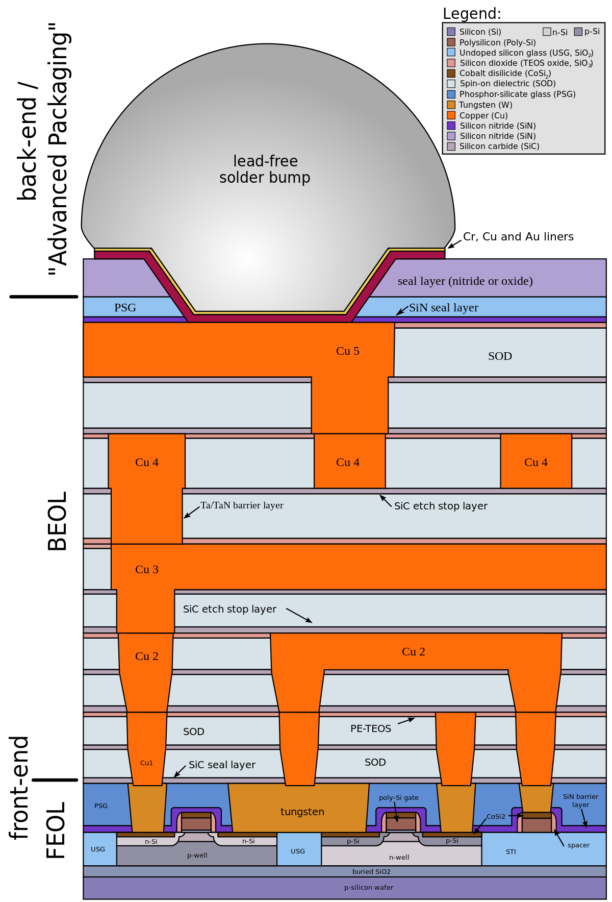
Wow, color me perplexed! I would have thought EUV on FEOL would be far more important. So, it must really be about mask sets more than anything else right now.Correct. For example Intel's Meteor Lake will use EUV mostly for the back end of line (BEOL) portion of the chip. Intel doesn't have enough EUV machines to make the whole chip with EUV.
View attachment 54377
Back end of line - Wikipedia
That said, I don't see how Fabs will be able to push GAA without EUV; which could just be my lack of understanding and imagination.
BorisTheBlade82
Senior member
Yes, he surely does, that I am totally convinced of. Look at his personal history - he is pretty much the human incarnation of the company.Intel must have promised to make him a billionaire or something. Or he just loves Intel like he's said a few times in interviews.
A cool $100M in restricted stock just for starters. In addition to a net worth already in the 8 figure range: https://www.oregonlive.com/silicon-...ger-with-a-package-valued-at-116-million.htmlWow, color me perplexed! I would have thought EUV on FEOL would be far more important. So, it must really be about mask sets more than anything else right now.
That said, I don't see how Fabs will be able to push GAA without EUV; which could just be my lack of understanding and imagination.
dullard
Elite Member
I'm just parroting what Ian Cutress posted here under "2022 H2, Intel 4": https://www.anandtech.com/show/1682...nm-3nm-20a-18a-packaging-foundry-emib-foverosWow, color me perplexed! I would have thought EUV on FEOL would be far more important. So, it must really be about mask sets more than anything else right now.
That said, I don't see how Fabs will be able to push GAA without EUV; which could just be my lack of understanding and imagination.
Intel's reasoning is beyond my CPU knowledge. I suspect it is because the FEOL is still relatively large components in Intel 4. It isn't until Intel 3 where these are made high density.Intel earlier this year stated that its Meteor Lake processor will use a compute tile based on this process node technology, and the silicon is now back in the lab being tested. Intel expects a 20% performance per watt gain over the previous generation, and the technology uses more EUV, mostly in the BEOL.
That is cause of limits of litho. Despite being touted as savior of industry for a decade, EUV in its 0.33NA form does not really allow tigher features than good old 1+ NA DUV with multi patterning. Despite 193nm vs 13.5nm wavelengths, NA plays huge role.
So EUV has economical advantages of less masks, better yields and so on, but the features printed are not that smaller than what is possible with DUV. So when faced with already "tight" structure like SRAM, the scaling is barely 0.8 or so lately between TSMC 7nm and 5nm processes, cause DUV was like 40nm MMP and EUV limit according to https://semiengineering.com/gearing-up-for-high-na-euv/ is ~30nm. And after Intel debacle with pushing things too far, probably noone dares to bet the farm on testing exact limit in high volume, so it is probably 36nm in practice.
The only ways to move to smaller features are: multi patterned 0.33NA EUV or moving to high NA of 0.55 EUV. Both have their own challenges that were highlighted in article above.
There are always challenges. The industry will move to high NA EUV in a few years, and I'm sure higher NA EUV is being researched. The reason DUV lasted so long was because of immersion. Maybe they can make that work for EUV eventually, and extend its life as long as DUV's was extended.
The problem with shrinking SRAM cells is a FinFET limitation. They'll be able to increase SRAM density much better as they move to nanosheets and CFETs beyond that.
Unfortunately it is a distinct possibility that Gelsinger will only have 5 years as CEO. I sure wouldn't bet on it though since it's an arbitrary board decision and the only potential historical application of it would have been with Craig Barret who transitioned from CEO to chairman of the board at age 65. While perhaps not quite on the same level as those that preceded him, I'd say Craig Barret was still a solid Intel CEO. Far better than the trio that followed that ran Intel like any generic big business.I agree with much of this. But Gelsinger has 5 years to turn around Intel or it will be too late (plus the board will enforce the retirement requirement on him). So he is out there trying to get any favorable advantage he can before it’s game over. He has become the biggest PR man and lobbyist in the industry. He bashes TSMC while working with them at the same time. He's arguing against government subsidies for US based TSMC Fabs, even though it’s in the government’s interest to hedge their bets. Maybe he is not 'panicked', but there sure is a fire under his butt. It’s not his fault that Intel is in the predicament that they are. It's the BODs over the last ~20 years, who choose profits and vertical growth over excellence in their core business and appointed CEOs that would accomplish those goals.
The last CEO, who really understood what Intels was, what it’s strengths were and how those strengths needed to be upheld and advanced was Andy Grove.
I would note that there is one reason for Intel to receive preferential treatment on US subsidies - Intel's leading edge process is developed and deployed in the US first. TSMC's Arizona site is scheduled to start production in 2024... with a 5nm class process that'll be what, 3-4 years old at that point? Meanwhile Samsung is intentionally neglecting to mention what process their new fab in Texas is targeting. (Their existing Austin fab "primarily focuses on the production of 14nm and 28/32nm technologies".) I wouldn't be the least bit surprised if Taiwan and South Korea are imposing IP export restrictions in order to keep the most lucrative investments by TSMC and Samsung in country. So the real choice might be subsidizing Intel to keep US semiconductor production as close to the leading edge as Intel can manage, or subsidize the table scraps from TSMC and Samsung.
IntelUser2000
Elite Member
Gelsinger is the best candidate. But it's 50/50 now if it's enough, because Intel is a big company with 100K+ employees and turning that ship around is hard. And I don't mean turning around from "Netburst to Core 2", because the problems were likely infesting the company before that. A single good product line doesn't change it. I think the Netburst issue was pointing to bigger problems within the core of the organization.
Remember as amazing as Core 2 seemed to be, 3 years later Apple came with the Smartphones and shocked everyone. Intel should have been the vendor ready to manufacture chips for them. And I mean ready by having such little power efficient chips being sold in the market already.
Pat is the one that saved them from financial ruin with 486 when others were pushing the i960 or something. You need a lot of Gelsingers in the product manager line, and CEO Gelsinger at the top, because it's not a one man job. If it was a one man job, then the problem would have been solved.
This is different from AMD because they are much smaller. Physical distances start to matter too. I mean a company with less than 10 employees it takes 1 min to get everyone up to speed. Now try doing the same with 100 thousand. Then you need endless meetings that waste 1/3rd of the day.
TRENDING THREADS
-
 Discussion Zen 5 Speculation (EPYC Turin and Strix Point/Granite Ridge - Ryzen 9000)
- Started by DisEnchantment
- Replies: 25K
-
Discussion Intel Meteor, Arrow, Lunar & Panther Lakes + WCL Discussion Threads
- Started by Tigerick
- Replies: 25K
-
 Discussion Intel current and future Lakes & Rapids thread
- Started by TheF34RChannel
- Replies: 24K
-

-
