- Jun 1, 2017
- 5,248
- 8,463
- 136
It's a little less than 2 years since the thread on design changes in Zen 2. It's unfortunate that even a month before the public launch of the first Zen 3 chips we still don't get any meaty information, but with the event we at least got some rough outlines which areas were changed and what their impact is. I hope AMD will fill in the interested public come time.
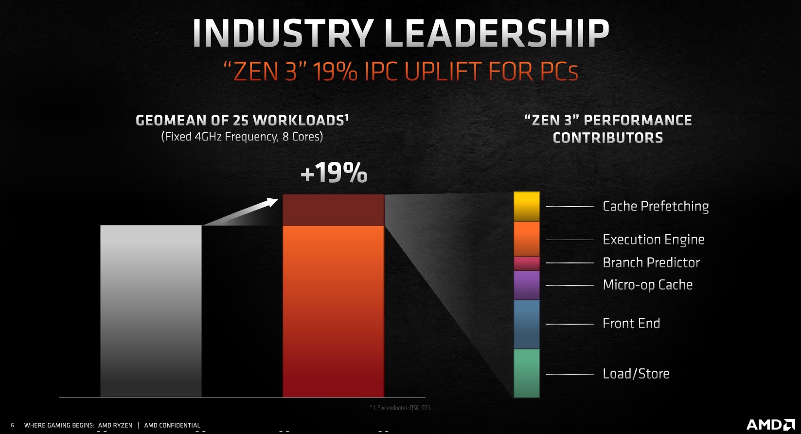
The 19% IPC improvement broken down into the different areas:
Doc used his pixel counting skill to come up with these numbers:
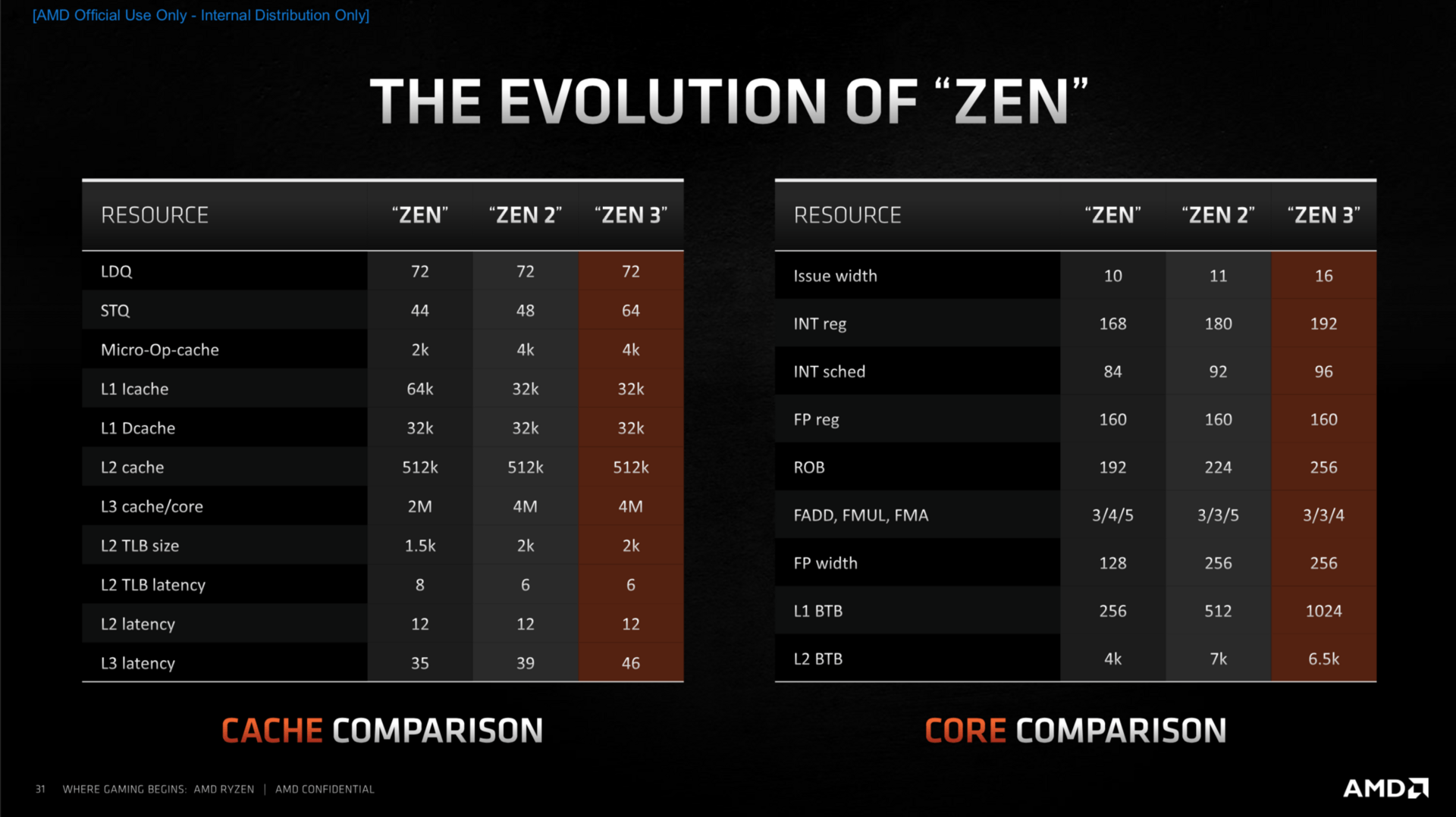
The first and essentially only Zen 3 leak, unified L3 cache per CCD, was confirmed:


More technical details to come, hopefully soon.
+2.7% Cache Prefetching
+3.3% Execution Engine
+2.7% Micro-op Cache
+4.6% Front End
+4.6% Load/Store
The 19% IPC improvement broken down into the different areas:
Doc used his pixel counting skill to come up with these numbers:
- +2.7% Cache Prefetching
- +3.3% Execution Engine
- +1.3% Branch Predictor
- +2.7% Micro-op Cache
- +4.6% Front End
- +4.6% Load/Store
The first and essentially only Zen 3 leak, unified L3 cache per CCD, was confirmed:
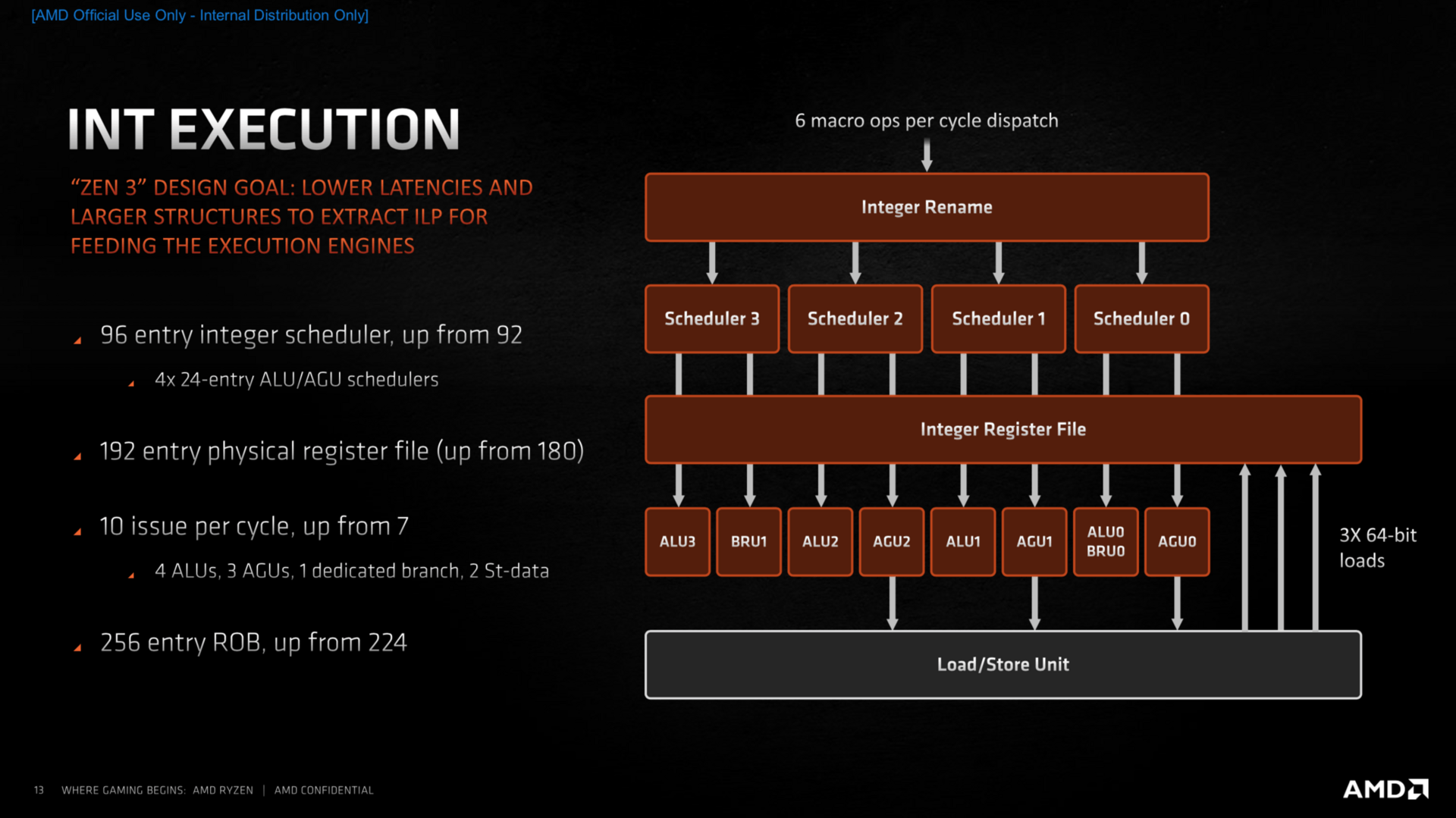
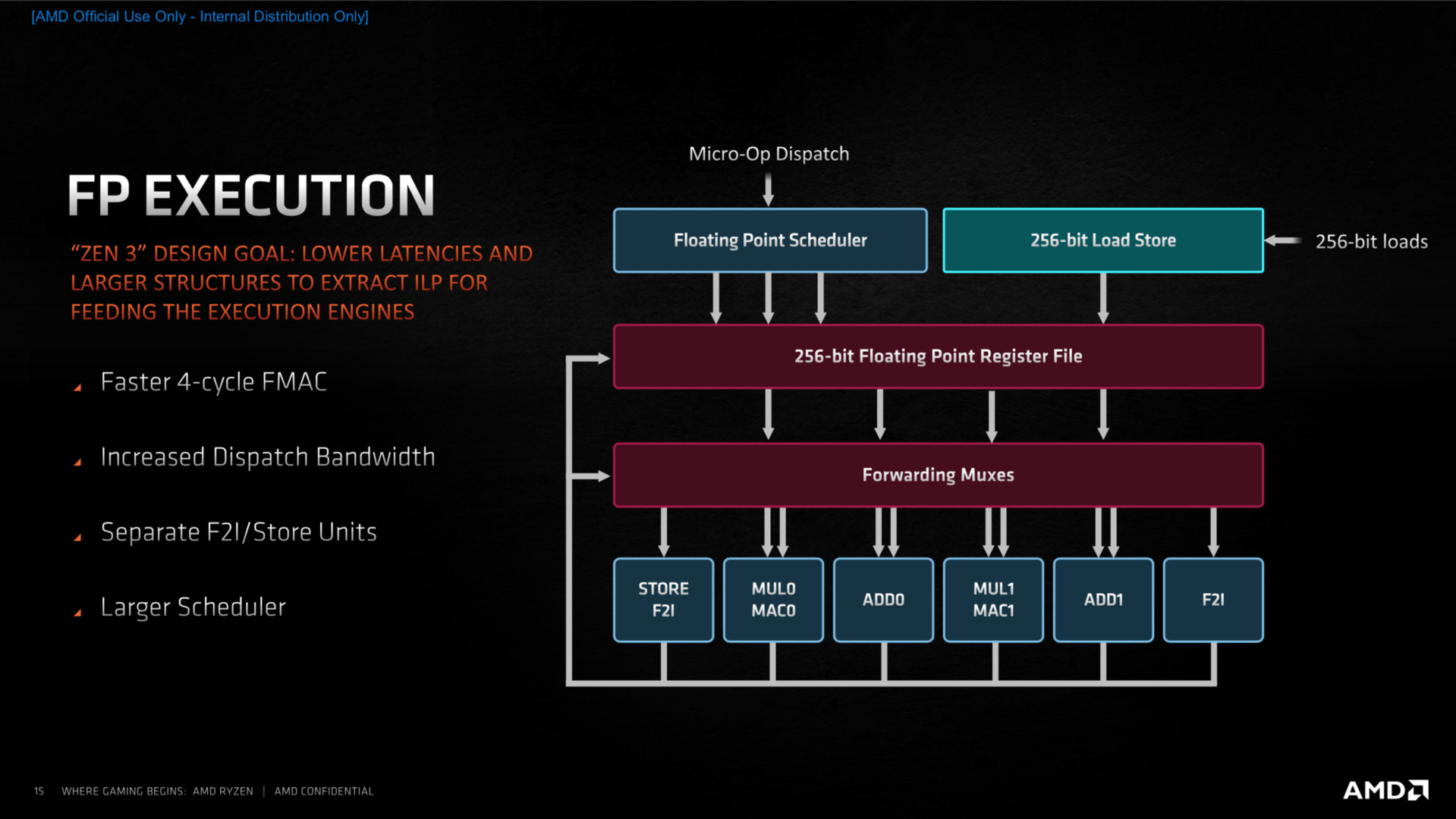
- Advanced Load/Store Performance and Flexibility
- Wider Issue in Float and Int Engines
- "Zero Bubble" Branch Prediction
More technical details to come, hopefully soon.
+2.7% Cache Prefetching
+3.3% Execution Engine
- "most likely an additional int unit and fp unit, taking it to 5x INT, 3x AGU, 3x FP" via #3
+2.7% Micro-op Cache
+4.6% Front End
+4.6% Load/Store
- higher Load/Store rate (Zen was 32B/cycle Load and 16B/cycle before while Intel Skylake featured double each) via #9
Last edited: