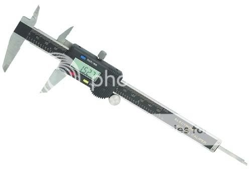
To answer one of the questions that is on many of our minds - "what is the gap between the CPU and the underside of the IHS?" - I took a bevy of measurements using a digital caliper that purports to have an accuracy of ±0.03mm (that's 30μm).
True to the enthusiast spirit of doing things as cheaply as possible, this is a
silly cheap caliper from Harbor Freight weighing in at an amazingly inexpensive $20

(I paid only $10 for it a few months ago it as a door-buster promo item). And despite its price, I was surprised it actually works as well as advertised, cheap as chips as it were.
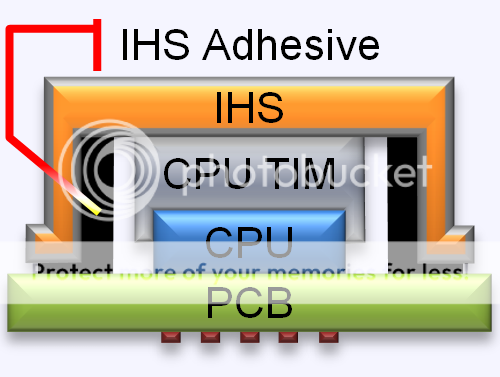
First, before we get into the measurements themselves, I felt we needed to establish some common-ground in terms of nomenclature so I don't confuse everyone (myself included). To that end, I created a goofy little drawing in powerpoint which I then overlaid in the pics to highlight what it is that I was measuring in that picture.
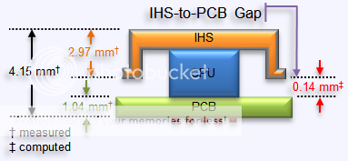
Here is our schematic for the cross-section of the IB CPU package - note absolutely nothing is to scale, the sizes are NOT relative. I just sized everything so the labels were legible, for example the CPU TIM isn't really that thick compared to the CPU, etc.
So you can see what I refer to as the "PCB", it is the green part of the CPU package that the CPU is connected to from above, and the LGA pads are underneath, with the capacitors (not labeled) located directly under the footprint of the CPU silicon die.
Also we see what I refer to as the "CPU TIM" being the thermal interface material located between the CPU silicon die and the underside of the IHS.
Likewise I refer to the black rubbery adhesive layer that binds the IHS to the PCB as "IHS adhesive".
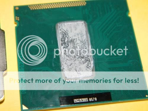
Now for the measurements, this is the full stack thickness as measured prior to the delidding but after I had lapped the IHS, I measure 4.21 mm:
Then I removed all the IHS adhesive (
detailed in this post) and all the CPU TIM from the CPU and the underside of the IHS, and restacked the IHS onto the PCB over the top of the CPU without any CPU TIM.
One of the questions we want to answer is "with the IHS adhesive removed, is there a gap between the CPU and the underside of the IHS for more CPU TIM to occupy or is the gap between the IHS and the PCB because the IHS itself is resting on top of the CPU?"
The resulting stack measured 4.15 mm, 0.06 mm thinner than the initial thickness:
From these measurements we see that the IHS adhesive that binds the IHS to the PCB must have lifted the IHS off of the PCB by at least 0.06 mm. (at this point we still don't know if the IHS is resting on the PCB or on the CPU die)
To answer this question we need to determine how shallow or deep the IHS recess is within which the CPU and CPU TIM reside. To make that measurement we must take two measurements and subtract them to arrive at the result.
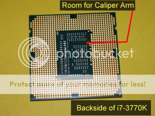
First, lets determine how thick (tall) the CPU die silicon is. To make this measurement I took advantage of the layout of the capacitors on the underside of the PCB, there is one little zone which I could snake the caliper tip into so the I got a good measurement of the CPU + PCB.
The CPU and the PCB weigh in at 1.57 mm, the result was repeatable, I remeasured it three times and it measured 1.57 mm each time.
^ notice how silly thin the CPU actually is, it barely sticks up above the PCB, by eye it looks like just a tiny little bump, perhaps half a millimeter.
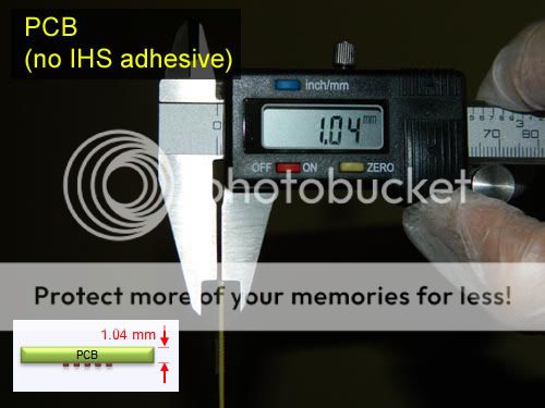
Next, measuring just the PCB's thickness, I get 1.04 mm:
This leaves us to conclude the CPU silicon die is a mere 0.53 mm thick (1.57 - 1.04). That is very thin.
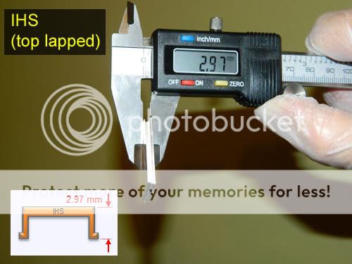
Next I measured the thickness of the IHS (this is after I lapped it, mind you), 2.97 mm:
(
due to a 10 image limit per post, the remainder of this post will be continued in the next post)