• We’re currently investigating an issue related to the forum theme and styling that is impacting page layout and visual formatting. The problem has been identified, and we are actively working on a resolution. There is no impact to user data or functionality, this is strictly a front-end display issue. We’ll post an update once the fix has been deployed. Thanks for your patience while we get this sorted.

Annotated hi-res core die shots of Zen 1 and 2

moinmoin

Diamond Member
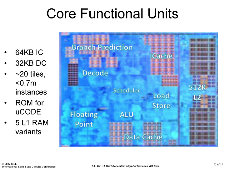
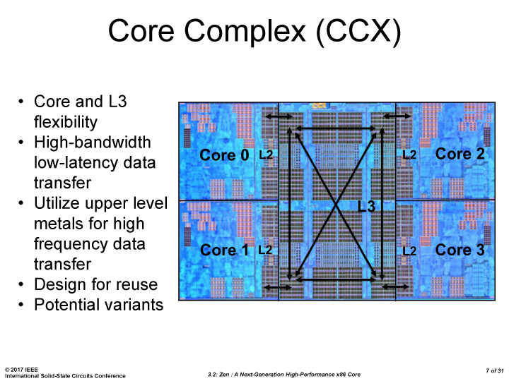
Sashleycat combined the recently revealed Zen 2 core annotation with Fritzchens Fritz's hi-res die shots, and added the Zen 1 core as well for comparison:

Zen 2 core:
5017e5_982e0e47d7c04dctkcg.jpg


Zen 1 core:
5017e5_727ef30243c547j9kue.jpg
 
Totally reelevant, but it is about the Matisse IO die (Also X570/TRX40).

They are claiming that there are 32 PCIe Lanes and that 4 of them are perhaps hardwired as SATA, giving a total of 28 usable PCIe Lanes. I believe that we will see that much in a Zen 2 based EPYC Embedded, which I'm currently speculating about at another place.
Note that while I have absolutely no real idea about how to read these die photos, due to the fact that previous Zeppelin Zen die had 4 10G MACs, I believe that these are still present in the Matisse IO die in order to have a feature parity with the previous EPYC Embedded line. What I believe is than what that website analysis consider 4 USB 3.1 Ports are morely likely to be the 4 10G MACs, and the 12 USB 2.0 are actually all identical USB Ports, with 4 capped to 2.0 speeds. It makes sense to me that it would be a more homogenous design than if there were two different types of USB Ports in silicon.
 
These two shots are not of complete dies but only the areas occupied by a single core (without L3 cache). You are talking about the uncore/IO portions.
Precisely, I'm talking about the ones from the link I provided. Your photos are annotated, it is easy to imply that they're a single Core.
 
Die shots have always fascinated me, but I can never wrap my head around them. Features like the various caches are super easy to pick out, but I have no idea how people identify the other parts.
 
Die shots have always fascinated me, but I can never wrap my head around them. Features like the various caches are super easy to pick out, but I have no idea how people identify the other parts.
This is why it's always nice to get official annotation like in this case.
(Note that only the Zen 2 core appears to be officially annotated, the Zen 1 core appears to be based on fuzzy guesses by WikiChip that Sashleycat cleaned up by comparing with the Zen 2 core annotation.)
 
Last edited:
Note the extensive use of synthesized logic in both designs compared to Intel's stubborn insistence of semi-custom functional blocks even with Sunny Cove.

This is why AMD can now iterate far quicker than the methodology challenged dinosaurs at Intel.
Humans love ordered stuff, don't we?
 
This is why it's always nice to get official annotation like in this case.
(Note that only the Zen 2 core appears to be officially annotated, the Zen 1 core appears to be based on fuzzy guesses by WikiChip that Sashleycat cleaned up by comparing with the Zen 2 core annotation.)


Zen1 was officially annotated in a hotchips presentation. Pretty sure the wiki version matches it
 
I see. We don't happen to have the slides of that publicly available, do we?

found it


and Sorry , was ISSCC not Hot Chips
 
Note the extensive use of synthesized logic in both designs compared to Intel's stubborn insistence of semi-custom functional blocks even with Sunny Cove.

This is why AMD can now iterate far quicker than the methodology challenged dinosaurs at Intel.

synthesized logic -> semi-custom
Intel typically is using full-custom flow for parts of the design.
 
Die shots have always fascinated me, but I can never wrap my head around them. Features like the various caches are super easy to pick out, but I have no idea how people identify the other parts.

Some of it comes down to having looked at or studied a lot of other examples, because even though there's going to be changes and shifts in each processor, the overall architecture isn't going to undergo radical redesigns so you know what to expect. Any company that did do something completely new would be hyping it up so anyone paying attention would know to look for it. Otherwise the standard pipeline stages are pretty well defined and everyone knows what should be there.

You can also block sections off based on where and how more prominent features are placed. The chip layout isn't going to have some winding border like a river or try to cram logic into every available crevice possible. Instead you'll get more clearly demarcated boundaries and some padding. Parts like the various caches especially tend to get laid out quite neatly which makes it easy to distinguish where the other parts are at.

Finally, some parts are just going to be physically located next to other parts because it makes it easier for them to communicate with other parts of the chip that they'll need to interact with most frequently. For example, you're going to want both the ALU and SIMD to have easy access to the data cache instead of having those all on opposite ends of the chip.
 
Back
Top