AMD Ryzen 5 2400G and Ryzen 3 2200G APUs performance unveiled

Page 48 - Seeking answers? Join the AnandTech community: where nearly half-a-million members share solutions and discuss the latest tech.

LTC8K6

Lifer
Mar 10, 2004
28,520
1,575
126
It's only 4C8T, shouldn't it have one CCX?
It should, but I see that's not the way AMD went.

In any case, the two CCX penalty seems to be much smaller than initially feared and I doubt it will make any difference.
 

Topweasel

Diamond Member
Oct 19, 2000
5,436
1,654
136
It's only 4C8T, shouldn't it have one CCX?
Are we talking about the 2400G? If so yes all RR's are 1CCX One 11CU Vega.

950px-raven_ridge_die_%28annotated%29.png
 
Last edited:

LTC8K6

Lifer
Mar 10, 2004
28,520
1,575
126
Are we talking about the 2400G? If so yes all RR's are 1CCX One 12CU Vega (11 is fully featured, the one is for yields).

950px-raven_ridge_die_%28annotated%29.png
No, the R5-1400, it has two CCXs, though it only has 4 cores.

I wonder if the extra load of the graphics systems on the infinity fabric will affect CPU performance?
 
  • Like
Reactions: french toast

Topweasel

Diamond Member
Oct 19, 2000
5,436
1,654
136
No, the R5-1400, it has two CCXs, though it only has 4 cores.

I wonder if the extra load of the graphics systems on the infinity fabric will affect CPU performance?
Why does the r5- 1400 configuration matter? As for IF and GPU who knows. It's probably a lot more bandwidth between the iGPU and the Modules in Carizzo, but there isn't going to be cross CPU core talk accross that so really it's going to come down to power. These will hit thermal limits well before the GPU can saturate performance over the bus if the CPU is needing to do work as well. Maybe we might see some diminishing returns when overclocking? But its not like the CPU is doing cross CCX pings to the GPU, there really shouldn't be the case of the CPU needing to use the cross CCX IF (well from CPUm to GPUm IF) bus unless its for work the GPU needs the CPU to do. So I'd doubt IF saturation is going to be an issue.
 

piesquared

Golden Member
Oct 16, 2006
1,651
473
136
I wonder what kind of CPU overclocks Ryzen G will obtain. At 65W there should be plenty of TDP headroom available for overclocking both Vega and Zen.
 

The Stilt

Golden Member
Dec 5, 2015
1,709
3,057
106
I wonder what kind of CPU overclocks Ryzen G will obtain. At 65W there should be plenty of TDP headroom available for overclocking both Vega and Zen.

Ryzens have OC-Mode which automatically activates once you increase the frequencies.
OC-Mode disables all power limiters.
 

Topweasel

Diamond Member
Oct 19, 2000
5,436
1,654
136
Infinity Fabric has to be the most molested term in the history of CPUs.
People are referring every single bus inside Zen based designs as IF.

It's no different than calling every single piece of electrical wire or cable as RJ-45.
Blame that on on AMD. Literally every connecting bus inside and outside is defined as IF by AMD.

1495056288_307_amd-plans-to-release-cpus-zen-2-zen-3-rome-milan-and-euv.png
 
  • Like
Reactions: psolord

The Stilt

Golden Member
Dec 5, 2015
1,709
3,057
106
Blame that on on AMD. Literally every connecting bus inside and outside is defined as IF by AMD.

1495056288_307_amd-plans-to-release-cpus-zen-2-zen-3-rome-milan-and-euv.png

That is an oversimplified overview, which is entirely correct (for the IF description).
It shows the connection between the CPU dies on the same substrate (GMI) and between the sockets (xGMI).

My rant was about the fact that people assume everything else is IF as well.

But true, AMD hasn't released much information to the public.

"Less is more" doctrine, unfortunately.
 

Topweasel

Diamond Member
Oct 19, 2000
5,436
1,654
136
That is an oversimplified overview, which is entirely correct (for the IF description).
It shows the connection between the CPU dies on the same substrate (GMI) and between the sockets (xGMI).

My rant was about the fact that people assume everything else is IF as well.

But true, AMD hasn't released much information to the public.

"Less is more" doctrine, unfortunately.

Again there is more that goes into detail of the CCXs themselves. They label the Mesh inside the CCX as IF as well. I think the bigger issue is just everyone assuming that the IF connection across CCX/Modules is going to be the cause of whatever missing performance numbers people want think they should hit and that it's as easy as AMD flipping a switch to make up for it. The problem is that GMI covers a lot of ground. Like intra-CCX mesh. Meaning any change that they might do to speed up the cross CCX communication would have major ramifications on intra CCX performance, stability, and yields. On top of that even if you could separate it out, this IF/GMI lane is for inter CCX mesh, this one for Module to module, then differ the xGMI on top of that to maximise throughput, do you even want to? I mean this is supposed to be a universal protocol to allow AMD to basically mix and match modules and dies that support it as they need to. Do you really add more complexity to that and make it that much harder to be universal just to eak out another 5 FPS in 1080p gaming.
 

raghu78

Diamond Member
Aug 23, 2012
4,093
1,475
136
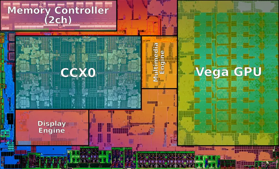
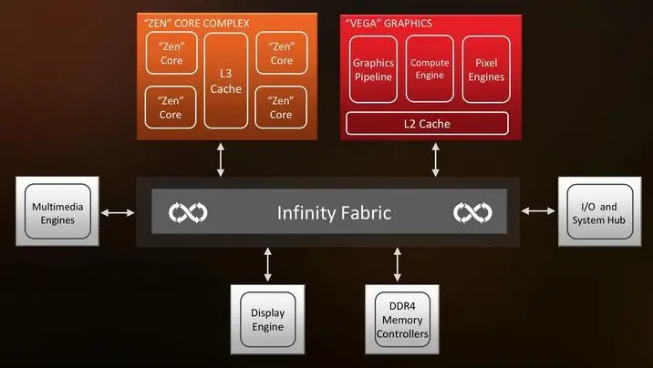
With respect to memory bandwidth contention as compared to the most recent Bristol Ridge chips, please remember that Ryzen G has an actual L3 cache (4MB to be precise). This will make a significant difference in the behavior of the memory controller. The flip side will be that, in the full fat Ryzen 5Gs with 4 cores and 8 threads, there can be 8 active threads all clamoring for memory bandwidth at the same time, which will definitely hit the L3 cache hard.

All that said, there will still be a major bottleneck with respect to memory bandwidth. I firmly believe that we will see a significant performance uplift over Bristol Ridge given the increased efficiency of the core internals, especially when considering thermal and power budgets, but, the lack of a major improvement in memory bandwidth will still put an absolute limit on higher resolution performance that will be unacceptable to many. While I realize that AMD has a still very limited R&D budget, I think that it would have been worth their while to consider cutting the CUs down to 8, expanding the die size by 20%, and including a roughly 128MB L4 cache to further help with memory bandwidth contention issues. We've already seen that this approach can make a noticeable improvement in iGPU performance from Intel's IRIS Pro products, and it could have done the same here. I also realize that it would have increased the cost of the chips by a non-trivial amount and would likely make them all at least 20% more expensive. I would take a 2200G that cost $125 over $99 and a 2400g that was a bit over $200 if it offered performance that was solidly past 1030/RX550 performance levels and nearing RX560 levels.

There is no point in AMD spending die size on EDRAM based L4 cache. The truth is the AMD APU will reach its full potential with a HBM cache and that is not yet possible because HBM2 memory and packaging tech is not cost effective and not yet high volume to be shipped in millions of mainstream APUs. I think by 2020 when the 7nm APUs arrive we will see AMD add a 2 or 4GB HBM2 cache and that would basically obsolete the 100-120 sq mm dGPU even with GDDR5 or GDDR5X. The way I see it AMD will achieve the complete realization of Fusion and Vision 25x20 vision by 2020. The AMD APU with HBM will be a truly disruptive product and will shrink the market for dGPUs significantly.
 
Last edited:
  • Like
Reactions: DarthKyrie

The Stilt

Golden Member
Dec 5, 2015
1,709
3,057
106
Again there is more that goes into detail of the CCXs themselves. They label the Mesh inside the CCX as IF as well. I think the bigger issue is just everyone assuming that the IF connection across CCX/Modules is going to be the cause of whatever missing performance numbers people want think they should hit and that it's as easy as AMD flipping a switch to make up for it. The problem is that GMI covers a lot of ground. Like intra-CCX mesh. Meaning any change that they might do to speed up the cross CCX communication would have major ramifications on intra CCX performance, stability, and yields. On top of that even if you could separate it out, this IF/GMI lane is for inter CCX mesh, this one for Module to module, then differ the xGMI on top of that to maximise throughput, do you even want to? I mean this is supposed to be a universal protocol to allow AMD to basically mix and match modules and dies that support it as they need to. Do you really add more complexity to that and make it that much harder to be universal just to eak out another 5 FPS in 1080p gaming.

In the picture you posted AMD didn't specify the internal structure of the core.
The overview is for EPYC MCM4 topology ("CPU" being a whole Zeppelin die).

Inside the Zeppelin die there are two major links we're interested in.
The controller fabric (SCF) and the data fabric (SDF).

The CCXs are connected directly to both of these fabrics.
The parts of the die which usually would be considered to belong to peripherals (USB, SATA, Ethernet, PCIe) are directly connected to the SCF and indirectly to the SDF (through IO Hub / IOMMU).

The memory controllers are connected to SDF only, as are the "SPDD" GMI connections used for MCM communication.
Meanwhile the xGMI links which are used to communicate between different packages as connected to both SCF and SDF.

Essentially the SDF is the same exact thing as the "northbridge" was in the previous designs, or at least serves the same purpose.
 

itsmydamnation

Platinum Member
Feb 6, 2011
2,743
3,075
136
Essentially the SDF is the same exact thing as the "northbridge" was in the previous designs, or at least serves the same purpose.
But its worth pointing out it performs nothing like the north bridge found in bulldozer. the north bridge connected the modules together and inter module latency was terrible..........
 

The Stilt

Golden Member
Dec 5, 2015
1,709
3,057
106
But its worth pointing out it performs nothing like the north bridge found in bulldozer. the north bridge connected the modules together and inter module latency was terrible..........

I don't recall BD having issues with the communication between the CUs.
At least no-one ever even mentioned it, as far as I can recall.

Maybe the hideous overall performance concealed that too well.
 

LightningZ71

Golden Member
Mar 10, 2017
1,627
1,898
136
There is no point in AMD spending die size on EDRAM based L4 cache. The truth is the AMD APU will reach its full potential with a HBM cache and that is not yet possible because HBM2 memory and packaging tech is not cost effective and not yet high volume to be shipped in millions of mainstream APUs. I think by 2020 when the 7nm APUs arrive we will see AMD add a 2 or 4GB HBM2 cache and that would basically obsolete the 100-120 sq mm dGPU even with GDDR5 or GDDR5X. The way I see it AMD will achieve the complete realization of Fusion and Vision 25x20 vision by 2020. The AMD APU with HBM will be a truly disruptive product and will shrink the market for dGPUs significantly.

At this point, I completely agree. Several years ago when RR was still being developed, which is when AMD was at it's most resource limited, if they could have figured out a way to do it with the resources they had, it would have been a solid decision. Now, with HBM2 further along, and the Intel/AMD collaboration chip in production, it would no longer be relevant.

However, I don't see the normal DDR based APU going away. It will continue to be a relevant, low cost alternative for the bottom of the product stack on SFF desktops and low end laptops/convertibles. There will just be a second step up that has a multi-chip-package like the KL-G product that will serve the middle of the market. At the top end, there still might be a place for a dGPU solution.
 

whm1974

Diamond Member
Jul 24, 2016
9,460
1,570
96
There is no point in AMD spending die size on EDRAM based L4 cache. The truth is the AMD APU will reach its full potential with a HBM cache and that is not yet possible because HBM2 memory and packaging tech is not cost effective and not yet high volume to be shipped in millions of mainstream APUs. I think by 2020 when the 7nm APUs arrive we will see AMD add a 2 or 4GB HBM2 cache and that would basically obsolete the 100-120 sq mm dGPU even with GDDR5 or GDDR5X. The way I see it AMD will achieve the complete realization of Fusion and Vision 25x20 vision by 2020. The AMD APU with HBM will be a truly disruptive product and will shrink the market for dGPUs significantly.
I don't think so as 2GB to 4GB is petty much entry level for games. Fine you just want to play at 1080p, but more gamers are wanting 4K. And such an APU will cost just as much as CPU and dGPU together.
 
  • Like
Reactions: PeterScott

itsmydamnation

Platinum Member
Feb 6, 2011
2,743
3,075
136
I don't recall BD having issues with the communication between the CUs.
At least no-one ever even mentioned it, as far as I can recall.

Maybe the hideous overall performance concealed that too well.
Nope inter module performance was amazingly bad, you would get random blow outs in latency between modules, by amd's own description there was a FIFO Service queue between modules. im guessing if you got stalls/needed cache flushes etc on the current transfer it got bad for the rest......

im guessing the whole write through L1 -> WCC -> L2 doesn't help that either. the new cache design is significantly better, Small contained domains that are directly accessible ( from a hierarchical point of view)
 

moinmoin

Diamond Member
Jun 1, 2017
4,933
7,619
136
In the picture you posted AMD didn't specify the internal structure of the core.
The overview is for EPYC MCM4 topology ("CPU" being a whole Zeppelin die).

Inside the Zeppelin die there are two major links we're interested in.
The controller fabric (SCF) and the data fabric (SDF).

The CCXs are connected directly to both of these fabrics.
The parts of the die which usually would be considered to belong to peripherals (USB, SATA, Ethernet, PCIe) are directly connected to the SCF and indirectly to the SDF (through IO Hub / IOMMU).

The memory controllers are connected to SDF only, as are the "SPDD" GMI connections used for MCM communication.
Meanwhile the xGMI links which are used to communicate between different packages as connected to both SCF and SDF.

Essentially the SDF is the same exact thing as the "northbridge" was in the previous designs, or at least serves the same purpose.
Always liked this chart for an overview how Zeppelin is set up internally.
kYmcYod.png
 

raghu78

Diamond Member
Aug 23, 2012
4,093
1,475
136
I don't think so as 2GB to 4GB is petty much entry level for games. Fine you just want to play at 1080p, but more gamers are wanting 4K. And such an APU will cost just as much as CPU and dGPU together.

Firstly AMD have designed Vega architecture to use a High bandwidth cache (HBC) and the memory utilization is better compared to earlier designs. I think by 2020 it will be cost effective to provide 4GB of HBC and it will perform like 6-8 GB VRAM. Obviously HBCC is a new technology and will improve the next few years and become a more robust and consistent solution. btw if you want to play at 4K you need to get a GTX 1080 Ti ideally or atleast a 1080 / Vega 64. 4K is not going to happen even on a $200 - 250 dGPU atleast if you are aiming at high settings and 40+ fps.
 
  • Like
Reactions: DarthKyrie

Shivansps

Diamond Member
Sep 11, 2013
3,835
1,514
136
Firstly AMD have designed Vega architecture to use a High bandwidth cache (HBC) and the memory utilization is better compared to earlier designs. I think by 2020 it will be cost effective to provide 4GB of HBC and it will perform like 6-8 GB VRAM. Obviously HBCC is a new technology and will improve the next few years and become a more robust and consistent solution. btw if you want to play at 4K you need to get a GTX 1080 Ti ideally or atleast a 1080 / Vega 64. 4K is not going to happen even on a $200 - 250 dGPU atleast if you are aiming at high settings and 40+ fps.

Remember that they need to keep a balanced price/performance here, at this point AMD should aim for a good 1080p game experience and nothing more, the $170 of the 2400G is already too much, they just cant increase prices anymore.
 

Insert_Nickname

Diamond Member
May 6, 2012
4,971
1,691
136
Remember that they need to keep a balanced price/performance here, at this point AMD should aim for a good 1080p game experience and nothing more, the $170 of the 2400G is already too much

How? They are giving you a 1500X equivalent, and throwing in a free IGP. I'd call that fair pricing.

For budget there is still the $99(!) 2200, but that one is insane value.
 

LTC8K6

Lifer
Mar 10, 2004
28,520
1,575
126
How? They are giving you a 1500X equivalent, and throwing in a free IGP. I'd call that fair pricing.

For budget there is still the $99(!) 2200, but that one is insane value.
1500X is probably faster than the 2400G CPU. It has it's own 65W envelope, it's own memory bandwidth, and 4X the L3 cache.