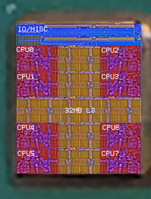
Here's a stupid question: do we even know for sure there is 32 MB L3 cache per chiplet?
I ask because it may be possible that there is no L4 cache in the IO chiplet and what there is instead is 256 MB centralized L3 cache instead, divided into 32 MB chunks: 1 per chiplet. If this is the case, then communication between the chiplets is only done within the IO chiplet and there is virtually zero latency there. On the other hand, there is the latency from the communication of CCX - IO - CCX, which is still unknown.
Think this way, moving data is expensive (power), executing data is rather cheap.
Moving inter chip is going to be a lot more expensive then intra chip.
Having to figure out where a line of memory is across many chips would be super expensive ( latency and power)
Now what you have is a trade off for each cache between, power usage, clocks, latency and Size. Each extra cache you add will increase latency. So all things being equal making the L3 twice the size has a cost, having an L4 has a cost. But moving the memory controllers into the I/O die has a cost(inter chip transfer).
It makes the most sense to have as much cache as possible within the chiplet, it make the most sense to track memory (tags) within the last cache within the chiplet (
@JoeRambo covered some options) . It then also makes sense to track which chiplet has what memory within the I/O die. As to weather an L4 is worth it, thats hard to tell, I do agree the I/O die doesn't seem big enough for an L4 cache, but it could still have a very large amount of Sram.
Even if you had an L4 thats fully inclusive on the I/O die that doesn't solve/ make memory requests between chiplets uniform. It infact makes the cache coherency protocol very complex. There will always be an extra cost going inter chiplet, its just were and how you pay for it(latency, power, total memory throughput).
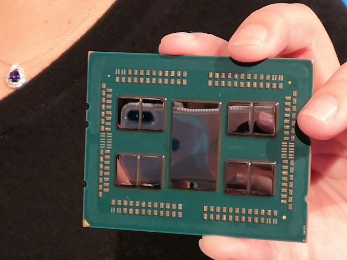
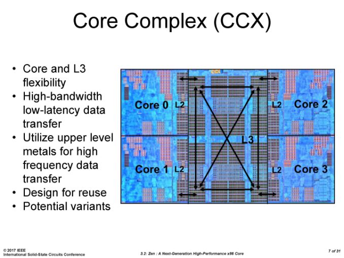
Any idea yet how the 8 cores are arranged within the CCX? I'd guess in a 3 by 3 grid, with the middle one missing:
The CCX chiplets do seem to be a perfect square, no?
They aren't square, There will be more on a chiplet then just the Cores and Cache, there is still the IF I/O, clock gens, management systems, i wonder if memory decryption will happen within a chiplet or in the I/O die etc.
The Core arrangement will be dictated by the interconnect technology,
2x 4core CCX == two squares like Zepplin
A ring bus would equal one big square of 4x2
a full mesh single CCX seems highly unlikely but a 4x2 arrangement seems most likely.