-
We’re currently investigating an issue related to the forum theme and styling that is impacting page layout and visual formatting. The problem has been identified, and we are actively working on a resolution. There is no impact to user data or functionality, this is strictly a front-end display issue. We’ll post an update once the fix has been deployed. Thanks for your patience while we get this sorted.
You are using an out of date browser. It may not display this or other websites correctly.
You should upgrade or use an alternative browser.
You should upgrade or use an alternative browser.
Question Zen 6 Speculation Thread
Page 230 - Seeking answers? Join the AnandTech community: where nearly half-a-million members share solutions and discuss the latest tech.
To showcase your technology and also future proofness (maybe Zen 6 with 700W and Zen 7 with 1000W, but you can keep your cooling solution infrastructure) such diagrams are helpful.These very clearly show SP7 1400W, with no mention of SP7, 700W or dual SP7, 1400W.
But I doubt that a single socket SP7 Zen 6 CPU will be operated at those power levels. It is inefficient and therefore the end of cost effective operation.
Markfw
Moderator Emeritus, Elite Member
Considering how many cores, it may still be efficient. We need to see power per core of Zen 4,5,6 to decide this question, its not JUST about pure power numbers. Having 512 cores could be the reason. (or more)To showcase your technology and also future proofness (maybe Zen 6 with 700W and Zen 7 with 1000W, but you can keep your cooling solution infrastructure) such diagrams are helpful.
But I doubt that a single socket SP7 Zen 6 CPU will be operated at those power levels. It is inefficient and therefore the end of cost effective operation.
adroc_thurston
Diamond Member
it's 600W.But I doubt that a single socket SP7 Zen 6 CPU will be operated at those power levels
Josh128
Banned
Mostly likely not a normal use case, but definitely single socket, not dual. The hidden nugget here is that the 256 core can likely be pushed to 1400W with max OC, that may have something to do with the supposed 2nm frequency capabilities.To showcase your technology and also future proofness (maybe Zen 6 with 700W and Zen 7 with 1000W, but you can keep your cooling solution infrastructure) such diagrams are helpful.
But I doubt that a single socket SP7 Zen 6 CPU will be operated at those power levels. It is inefficient and therefore the end of cost effective operation.
Lisa Su:
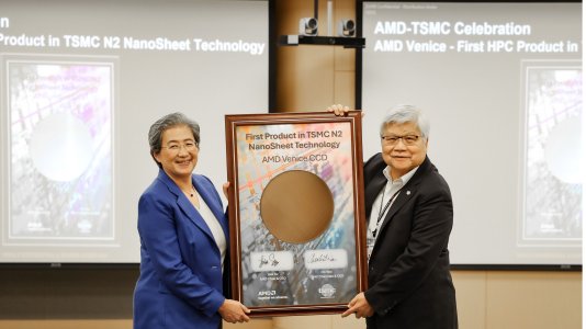
"Venice extends our leadership across every dimension that matters in the data center," said Lisa Su, chief executive officer of AMD. "More performance, better efficiency, and outstanding total cost of ownership. It is built on TSMC 2nm process technology and features up to 256 high performance Zen 6 cores. It delivers 70% more compute performance than our current generation EPYC 'Turin' CPU and and to really keep feeding [the Instinct MI400X accelerators] with data at full speed, at even at rack scale, we have doubled both the GPU and the memory bandwidth and optimized Venice to run at higher speeds. […] We just got 'Venice' back in the labs and it is looking fantastic."
From a couple months old Toms Hardware article:
AMD's 6th Generation EPYC processors are expected to adopt the all-new SP7 form-factor that is projected to enable the company to place more compute complex dies (CCDs) on the package, increase the number of memory channels, and boost peak power delivery well beyond 700W supported by the SP5 packaging.

AMD EPYC Venice boasts 256 cores and bandwidth galore — next-gen server CPUs arrive in 2026
Per-socket memory bandwidth is increasing to to 1.6 TB/s.
Last edited:

AMD's SP7 platform could enable CPUs with up to 1,400W of peak power consumption — chillers tested to keep heat in check
CPUs are going the way of GPUs?www.tomshardware.com
There was a tidbit from MLID that AMD has Venice Dense (256 core) running at base clock speed faster that full Zen 5 core boost clock, which sounded insane (not credible). But this could possibly explain it. And this would be a monster CPU.
adroc_thurston
Diamond Member
It's 600W socket power (well, a chunk of it is from 33% moar memory attached).There was a tidbit from MLID that AMD has Venice Dense (256 core) running at base clock speed faster that full Zen 5 core boost clock, which sounded insane (not credible). But this could possibly explain it. And this would be a monster CPU.
It's 600W socket power (well, a chunk of it is from 33% moar memory attached).
Semi-custom?
adroc_thurston
Diamond Member
No.Semi-custom?
You're reading too much into silly R&D stuff.
You all should stop.
I think MLID mixed up with the clock speed.There was a tidbit from MLID that AMD has Venice Dense (256 core) running at base clock speed faster that full Zen 5 core boost clock, which sounded insane (not credible). But this could possibly explain it. And this would be a monster CPU.
Turin Zen5 (N4P) 8-core 32MB vs Turin Dense Zen5c (N3E) 16-core 32MB:
All core: 4.1GHz vs 3.35GHz.
Boost clock: 4.1GHz vs 3.7GHz
Zen6 (N3P) 12-core 48MB vs Zen6c (N2) 32-core 128MB ?
Yep, I still think only Zen6c is fabbed by N2 node. Is MLID referring to Turin or desktop Zen5? Cause Turin Zen5 is able to boost up to 4.1GHz ???
adroc_thurston
Diamond Member
That's N2p.Zen6 (N3P) 12-core 48MB
N2P is not even HVM. And Venice is launching in 2026, not 2027.That's N2p.
adroc_thurston
Diamond Member
yeah it is, q3'26 ramp too.N2P is not even HVM.
Pretty much everything Zen6 not tied to gfx13 is 2026.And Venice is launching in 2026, not 2027.
Q3 26 ramp means mass availability in end of Q4 to Q1 27 as N2 plus packing takes like around 14-18 weeksyeah it is, q3'26 ramp too.
Last edited:
marees
Platinum Member
& zen 6 with RDNA 5 (medusa Premium & Halo — not counting consoles) is 2028 ?yeah it is, q3'26 ramp too.
Pretty much everything Zen6 not tied to gfx13 is 2026.
adroc_thurston
Diamond Member
yes, take your meds.
No, ramp in TSM words means volume wafers churning out until node is at capacity. Not Intel 'ramp' (a joke, really).3 26 ramp means mass availability in end of Q4 to Q1 27 as N2 plus packing takes like around 14-18 weeks
how the hell would it be 2028?& zen 6 with RDNA 5 (medusa Premium & Halo — not counting consoles) is 2028 ?
yes, take your meds.
Yep, buy new glass, old man. 😎
No, ramp in TSM words means volume wafers churning out until node is at capacity. Not Intel 'ramp' (a joke, really).
how the hell would it be 2028?
marees
Platinum Member
I believe that was a roadmap leaked by a board partner (which must have been shared to them by AMD)yes, take your meds.
No, ramp in TSM words means volume wafers churning out until node is at capacity. Not Intel 'ramp' (a joke, really).
how the hell would it be 2028?
adroc_thurston
Diamond Member
It didn't have MDSp/h on it.I believe that was a roadmap leaked by a board partner (which must have been shared to them by AMD)
They're under graphics.
Josh128
Banned
So what is the current generally accepted info about Zen 6 CCDs? The below is what I think is current leaks:
Desktop / non-dense / mobile chiplet based CCD/CCXs: 12 core / 12 core (3nm or 2nm?)
EPYC Dense CCD/CCXs: 32 core / 32 core (2nm)
Mobile monolithic CCXs : 12 core (3nm?)
Do we know anything about the desktop and mobile chiplet GPUIOD / GPULPCPUIOD process nodes? Im assuming 4nm or 3nm?

Desktop / non-dense / mobile chiplet based CCD/CCXs: 12 core / 12 core (3nm or 2nm?)
EPYC Dense CCD/CCXs: 32 core / 32 core (2nm)
Mobile monolithic CCXs : 12 core (3nm?)
Do we know anything about the desktop and mobile chiplet GPUIOD / GPULPCPUIOD process nodes? Im assuming 4nm or 3nm?

N2PDesktop / non-dense / mobile chiplet based CCD/CCXs: 12 core / 12 core (3nm or 2nm?)
N2PEPYC Dense CCD/CCXs: 32 core / 32 core (2nm)
N3PDo we know anything about the desktop and mobile chiplet GPUIOD / GPULPCPUIOD process nodes? Im assuming 4nm or 3nm?
Josh128
Banned
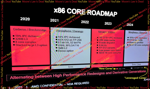
Its interesting to note (I just noticed this) that the end of the road map timeline is currently 2 years ahead of where we are now, assuming Zen 6 launches in fall of 2026, despite being only 11 months behind at the beginning when Zen 3 launched (Nov 2020).
Wonder if falling behind was due to TSMC, AMD, or Intel just not being competitive?
Wonder if falling behind was due to TSMC, AMD, or Intel just not being competitive?
This is Internal Roadmap not Public stuff can change in 2020 no one thought they would have to wait an extra year for usable N3 Process. N3B doesn't count cause only Apple and Intel got it no one else(Intel must have cried on the subpar performance vs N4P and delay as they went to TSMC due to no delays).Its interesting to note (I just noticed this) that the end of the road map timeline is currently 2 years ahead of where we are now, assuming Zen 6 launches in fall of 2026, despite being only 11 months behind at the beginning when Zen 3 launched (Nov 2020).
Wonder if falling behind was due to TSMC, AMD, or Intel just not being competitive?
ToTTenTranz
Senior member
A bit sad to see the iGPU being kind of relegated to a 2nd class citizen. At least with the Zen5 and previous monolithic APUs the iGPU would get access to the same process node.
TRENDING THREADS
-
Discussion Zen 5 Speculation (EPYC Turin and Strix Point/Granite Ridge - Ryzen 9000)
- Started by DisEnchantment
- Replies: 25K
-
Discussion Intel Meteor, Arrow, Lunar & Panther Lakes + WCL Discussion Threads
- Started by Tigerick
- Replies: 24K
-
Discussion Intel current and future Lakes & Rapids thread
- Started by TheF34RChannel
- Replies: 24K
-
-

