- Mar 3, 2017
- 1,779
- 6,798
- 136

No, it looks like a 16c CCX and two 4c CCX. The big questions:
View attachment 76892
- Are these really just 3 CCX on a custom die or 2 different types of CCD connected?
- Is the 16c CCD essentially Bergamo?
- Will Bergamo get rid of IFoP just as MI300 does?
- Will this be the little to Zen5's BIG?
Just the picture - annotations by AMD.
The 4x4 block just doesn't look anything like a CPU whereas, as @HurleyBird mentioned, the top and bottom sections look like 8 core CCXs. I realize it's not a true to life render, but the 4x4 section is not even really close to a CPU looking structure. Who knows though, I'm happy waiting until AMD actually reveals more details.
Zen 4c is also more cores per chiplet mind you.I think 24 CPU cores on Mi300 came from one of AMD's presentations (I don't remember which one).
As @DisEnchantment mentioned, Mike Clark has been talking about potentially more cores per chiplet, and as I mentioned before, this has to be a brand new, ground up new Zen 4 chiplet, which gets all of its power and IO from TSVs, it may just as well have the 12 cores.
The key point is the interconnect, which is completely different in MI300 than Epyc. Also Clark said more cores per L3 complex. So not 4c.Zen 4c is also more cores per chiplet mind you.
It has them split out across 2 CCXs, but is still double the cores per CCD.


Some napkin measurements, since Locuza has retired 😁
Width for what I suspect is a 16c CCD is 9.2mm, Height is 7.9mm, area is 73.0mm2.
- based on Locuza's measurements of a de-lidded MI300 and AMD's own rendering
- assuming, that at least proportions and aspect ratio on the render are accurate
Quite coincidentally what AMD has been saying about Bergamo: Double the cores, same area 😉
View attachment 76944
View attachment 76945
Why would they? AMD already stated 24c in total for MI300. And sizes for the two 2x2 blocks matches as well.Hmm... Could those 2 smaller chiplets fit 12 cores each? Assuming those chiplets would not have L3 cache or GMI links...
Well to nobody's surprise, patent trail is right again on the PIM. And with Samsung indeed. They started with Xilinx and extended to CPU. Posted patents again for context.However I noticed AMD has been working a lot on PIM, just a handful of what I found
I am wondering if the feature they had with Xilinx Virtex Ultrascale+ with Samsung Aquabolt XL for PIM will make it to Zen 5 DC parts with HBM (MI300 type parts), usually recurring patents and provisional patents are good candidates for making it to a product.
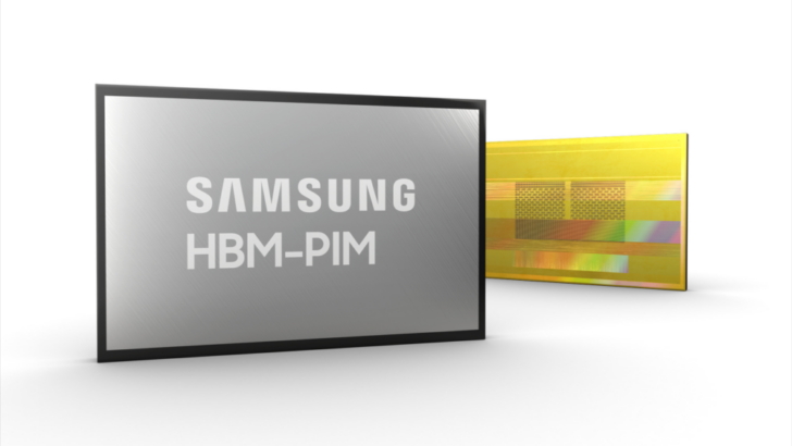
Samsung Brings In-Memory Processing Power to Wider Range of Applications
Integration of HBM-PIM with the Xilinx Alveo AI accelerator system will boost overall system performance by 2.5X while reducing energy consumption by more than 60% PIM architecture will be broadly deployed beyond HBM, to include mainstream DRAM modules and mobile memorynews.samsung.com
PROVIDING ATOMICITY FOR COMPLEX OPERATIONS USING NEAR-MEMORY COMPUTING
<https://www.freepatentsonline.com/y2022/0413849.html>
APPROACH FOR REDUCING SIDE EFFECTS OF COMPUTATION OFFLOAD TO MEMORY
<https://www.freepatentsonline.com/y2023/0004491.html>
ERROR CHECKING DATA USED IN OFFLOADED OPERATIONS
<https://www.freepatentsonline.com/y2022/0318089.html>
DETECTING EXECUTION HAZARDS IN OFFLOADED OPERATIONS
<https://www.freepatentsonline.com/y2022/0318085.html>
Processing-in-memory concurrent processing system and method
<https://www.freepatentsonline.com/11468001.html>
OFFLOADING COMPUTATIONS FROM A PROCESSOR TO REMOTE EXECUTION LOGIC
<https://www.freepatentsonline.com/y2022/0206855.html>
MEMORY ALLOCATION FOR PROCESSING-IN-MEMORY OPERATIONS
<https://www.freepatentsonline.com/y2021/0303355.html>
Command throughput in PIM-enabled memory using available data bus bandwidth
<https://www.freepatentsonline.com/11262949.html>
HARDWARE-SOFTWARE COLLABORATIVE ADDRESS MAPPING SCHEME FOR EFFICIENT PROCESSING-IN-MEMORY SYSTEMS
<https://www.freepatentsonline.com/y2022/0066662.html>
PROCESSOR-GUIDED EXECUTION OF OFFLOADED INSTRUCTIONS USING FIXED FUNCTION OPERATIONS
<https://www.freepatentsonline.com/y2022/0188117.html>
REUSING REMOTE REGISTERS IN PROCESSING IN MEMORY
<https://www.freepatentsonline.com/y2022/0206685.html>
PRESERVING MEMORY ORDERING BETWEEN OFFLOADED INSTRUCTIONS AND NON-OFFLOADED INSTRUCTIONS
<https://www.freepatentsonline.com/y2022/0206817.html>
Providing host-based error detection capabilities in a remote execution device
<https://www.freepatentsonline.com/11409608.html>
VIRTUALIZING RESOURCES OF A MEMORY-BASED EXECUTION DEVICE
<https://www.freepatentsonline.com/y2022/0206869.html>
MANAGING CACHED DATA USED BY PROCESSING-IN-MEMORY INSTRUCTIONS
<https://www.freepatentsonline.com/y2022/0188233.html>
DYNAMICALLY COALESCING ATOMIC MEMORY OPERATIONS FOR MEMORY-LOCAL COMPUTING
<https://www.freepatentsonline.com/y2022/0414013.html>
OPTICAL BRIDGE INTERCONNECT UNIT FOR ADJACENT PROCESSORS
<https://www.freepatentsonline.com/y2022/0318174.html>
FANOUT MODULE INTEGRATING A PHOTONIC INTEGRATED CIRCUIT
<https://www.freepatentsonline.com/y2022/0342165.html>
OPTICAL DIE-LAST WAFER-LEVEL FANOUT PACKAGE WITH FIBER ATTACH CAPABILITY
<https://www.freepatentsonline.com/y2022/0206221.html>
I think AMD rendering is not precise or purposefully vague. There should be some debug circuitry like the Debug circuity on the current CCD on the CCX top die in MI300.Some napkin measurements, since Locuza has retired 😁
Width for what I suspect is a 16c CCD is 9.2mm, Height is 7.9mm, area is 73.0mm2.
- based on Locuza's measurements of a de-lidded MI300 and AMD's own rendering
- assuming, that at least proportions and aspect ratio on the render are accurate
Quite coincidentally what AMD has been saying about Bergamo: Double the cores, same area 😉
View attachment 76944
View attachment 76945

I am trying to perform this exercise regardless of how futile it may be. From Locuza, he measured 365mm2 for the base die.@DisEnchantment
Yes, I know. They simply photoshopped some "idealised" structure patterns together. But somehow I am under the impression that at least proportions and aspect ratio are the real deal - everything just adds up too nicely...

Is the 16c CCD essentially Bergamo?
The bigger chiplet in the middle (150mm2-160mm2) is likely XDNA.
You are right.@DisEnchantment
I just spotted an error in your calculation: You assume 365mm2 for the CPU block from Locuza. But he measured the structural silicon, which goes all the way from HBM to HBM. On the render there is a lot of area around the CPU structure - so you are overestimating the 4x4 structure and everything else. Please have a look again at the two pictures I posted for reference.

Well to nobody's surprise, patent trail is right again on the PIM. And with Samsung indeed. They started with Xilinx and extended to CPU. Posted patents again for context.
View attachment 76947
And on the optical interconnect seems to match patent again. Great potential on the using this for the next gen XGMI. Nice long reach interconnect for the unified memory architecture.
View attachment 76948
I am curious whether PIM will come in MI300A instead of Zen 5.
- AMD confirmed this whole sector to be the CPU part, they also confirmed 24 cores and there are 24 identical structures looking much like idealised cores. Isn't that a lot of evidence in and of itself? (edit: "indication" might be more appropriate)
[*]The middle die will not need structures like an iMC for Bergamo, because it has some form of IOD. MI300 has no IOD, that is why the custom die on top and bottom has something that looks like that.
Do you see PIM and HBM as exclusive choices? It's not, and allows further power reductions irrespective of the memory used.The PIM is nice, but I think it is a short run solution (which may lack some flexibility).
AMD already signaled (IMO) a long-term solution - HBM stacked on compute.
Well, not exactly, but imagine one of the quadrants of Mi300 with base die + 2 HBM stacks. Imagine enlarging the base die and stacking the HBM stacks on top of it.
So Mi300 maybe the first leg of realizing power savings going from:
DIMMs - 12 pj/bit
HBM with 2.5D, 2 jumps over microbumps = 3.5 pj/bit
Better than 3x improvement.
Suppose Mi400 has this arrangement of stacking HBM stacks on top of base die, the energy needed falls to 0.2 pj/bit. That being 60x improvement, or if 2 trips over Hybrid Bond are 0.2 each, then 0.4, and that would be exactly the 30x improvement in power that AMD has proposed over ~5 years.


now that the 7950X3D has launched, is that the end of the road for updates to consumer desktop Zen 4? And is it clear yet what kind of spec increases are on the horizon for Zen 5? I am looking for ways to fit the most capacity (CPU cores + memory) in a small form factor (mITX), and it seems like 7950X(3D) + 96GB (two-slot mITX) might be the best available for the next year or more. I am trying to figure out if we are expecting any Zen 5 offerings to significantly exceed that kind of capacity in the desktop space? More cores and/or more memory support?
Not very likely I think, diminishing returns for DT especially with faster DDR5.I think we will see more than 1 layer of V-Cache and maybe improved tolerances for the V-Cache so that the it cam be clocked closer to non-V-Cache Hopefully before Christmas of this year.
I also would like to see a 12 core CCD on N4P. But...the CCD is going to be large.On a low probability end of things, AMD may have a 12 core Zen Core CCD that can be stocked on top of base die. In theory, AMD could reuse this CCD and release a new client base die.
12C per L3getting more cores in a sharing L3 environment
L2 1MiB --> 1.5MiBThen the L2 - if your L2 is bigger then you can cut back some on your L3 as well.
Not very likely I think, diminishing returns for DT especially with faster DDR5.
I also would like to see a 12 core CCD on N4P. But...the CCD is going to be large.
View attachment 77369
Totally guessing based on Mike's statement's
12C per L3
L2 1MiB --> 1.5MiB
L3 4MiB/Slice --> 3MiB/Slice = 36MiB/CCD
GMI SerDes PHY replaced with a lower power PHY with small beach head.
A ring with quadrants would probably be suitable to cut latency across 12 cores. Additionally the faster interconnect should help when snooping the other CCX.
Even with this, CCD seems a bit too big for AMD, ~100mm2 is quite big. Unless, they manage to use the perf gains from N4P and claw back some density tradeoffs to reach at least ~90mm2.
On the other hand N4/5 supply is plenty in 2024, 180k+ wpm.
Additionally, the IOD will be totally new. RDNA3+ and AIE for DT as well.
Too much unknowns but interesting for me to ponder about this, as usual.
