- Mar 3, 2017
- 1,777
- 6,791
- 136

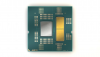
Not sure if this is widely known, Zen 5 is family 26/1Ah. Kernel patches are landing now.
It was just developed, It's only sample production for customers.
It will take time until It's available in first products, maybe in Q4 2023?
When Strix Point will arrive, then price could be lower, true, but It will be higher than lower clocked ones.
Strix with this memory would once more not be for cheaper laptops but premium ones.
I always thought APU was meant as a cheaper alternative to CPU+dGPU combo, yet It's not.
I am talking about laptops here.In upcoming years, it will be impossible to build DIY PC of entry level to mainstream level performance for equal or less amount of money as you would have to pay for Mini-PC, or APU based system.
Its not the problem with the dies and their prices. Its the problem of prices of everything around them: DRAM, GDDR memory, PCBs, controllers, power delivery, manufacturing costs of separate components.
"APU based system".I am talking about laptops here.
Didn't you notice how much they ask for Rembrandt laptops? Phoenix will end up the same and Strix too. Too expensive for that performance."APU based system".
I should also add to that: SOC based system.
Which one of Strix Point dies?Didn't you notice how much they ask for Rembrandt laptops? Phoenix will end up the same and Strix too. Too expensive for that performance.
")
What are the options? Rare, medium or well done?Which one of Strix Point dies?
All of them.What are the options? Rare, medium or well done?
I haven’t kept up on the mobile stuff, but I would expect PC laptop makers will need something to compete with the Apple M2 systems eventually, so high end APUs may be a thing eventually. A regular processor with a discrete gpu will not be able to compete on power consumption with a high end APU.Didn't you notice how much they ask for Rembrandt laptops? Phoenix will end up the same and Strix too. Too expensive for that performance.
Not sure if this is widely known, Zen 5 is family 26/1Ah. Kernel patches are landing now.
Hmmm, if we knew, when the Zen 4 Kernel patches came out, can we then get a feel for the rough potential launch window of Zen 5?
Zen 4 patches started appearing at the end of 2021.Hmmm, if we knew, when the Zen 4 Kernel patches came out, can we then get a feel for the rough potential launch window of Zen 5?
They more or less need to, if they want to keep the Mobile cadence with Strix Point.Zen 4 patches started appearing at the end of 2021.
Zen 1 and Zen 2 developed by first team
Zen 3 and Zen 4 developed by second team
AMD's newish cadence should be around 18 months and Zen 4 should have launched earlier, but Norrod postponed it by 2Q to add CXL.
I would say early 2Q24 should be the launch window considering the team developing Zen 5 is working in parallel.
Which makes it 18 Months after Zen 4 (if you add the additional 2Qs of Zen 4 push back that makes it two years from the supposed original Zen 4 planned launch, from Forrest Norrod's statement)
So, I would not be surprised if they launch Zen 5 at CES24
I suspect Zen5 will use some of the stacking and connectivity tech used for RDNA3 and MI300, so it is kind of relevant. The things you have labeled as Zen4 cores look more like infinity cache, or maybe L2 cache, or something like that. I have seen the small chips between the HBM3 referred to as structural silicon (semiaccurate, I think). The chiplet you have labeled as "adaptive chiplet" looks exactly like a Zen 4 chiplet with 8 cores. The thing you have labeled "AI chiplet" may be partially FPGA. FPGAs have large arrays, so it could look like cache. It could also just be all AI hardware. That would have large, regular, arrays of things in addition to possible caches. It would be easier to tell if I knew the die size of HBM3. I didn't find it in a quick search and I don't have time to search more today. I thought HBM2 was around 100 mm2. The rendering may be completely inaccurate, but if the "AI chiplets" are actually cpu cores, then where do the 24 cores come from? There are essentially 3 GPUs (2 chiplets each), so having 3x8-cores would make sense. I don't know where the other 8 cores would be hiding unless there is something weird like 2 low power cores in each base die.
Replying to myself...
I am wondering if the layout pictured just isn't the 24 core device. Perhaps it is a 16 core with an FPGA or other accelerator. They apparently can put more than one type of chip on top of the base die. The base die looks like it might be able to fit 4 cpu chiplets, so I am wondering if the 24 core variant is really the top end. This seems like a small number of cores compared to what Nvidia will have with each Grace Hopper package (144?), although that may have a more powerful gpu.
It looks like my speculation that the MCD could have v-cache stacked on top might be correct; don't know anything about this person though:
It makes it a lot simpler to manufacture if the base die (MCD) is the same size as the v-cache die. They can just do wafer on wafer without dicing and making a reconstituted wafer with cache die and small pieces of filler silicon. If something goes wrong, it is only an MCD die, not a more expensive cpu or gpu die/wafer. That should make it a lot cheaper, so I would expect MCDs to be used other places. MI300 doesn't seem to use them unless they are embedded under the compute die in some manner. I haven't seen anything about off package memory channels on MI300/SH5, but it seems like they would have extra memory somehow, unless they are depending on CXL with essentially HBM cache. HBM still has rather high latency though, since it is still DRAM, so I would expect cache to be under there somewhere. A single silicon interposer under the entire thing still seems too expensive and unnecessary. It seems like it would be smaller embedded die and/or EFB bridge chips.
Navi 31, 32 use the MCD chiplet to save on N5 die area and as means to make memory bandwidth a building block, to add more or less bandwidth, as needed per GPU model.
On Mi300, there is already a base die of less expensive N6, and the base die will always interface with 2 HBM stacks, so the memory controller will be a fixed implementation, that will be part of base N6 die. And the N6 die will likely have a lot of L3 SRAM for cache.
So not really any commonality / similarity between the RDNA 3 and CDNA 3 packaging of components, IMO.

We would prefer that AMD take its time and not do a hurried launch. It's the pesky investors that AMD has more trouble trying to satisfy.Here's hoping zen 5 isn't a half baked ham.
It isn't necessarily implemented as a single interposer under each group of 2 gpu chiplets. That would be quite large and expensive.
They have shown images kind of indicating infinity cache die embedded under the compute die:
This could just be illustrative; I can't rule out a giant interposer, but it seems like it would be something on the order of 200 to 300 mm2 per each 2 gpu chiplets? Does it need that much for an infinity fabric switch, caches, and whatever IO it has? Even at 200 mm2, that is more than 2x the size of an epyc genoa IO die if all 4 of them are considered. I think they are bigger than 200 mm2; the HBM stacks are over 100 mm2. The actual fabric switches are very small. They need wider connections for gpus, but the PHY is minimal for anything stacked.

@jamescox
With the little knowledge we have, GF is entirely possible. Intel uses some 14/22nm process for their MTL interposer. Some 16-10nm TSMC legacy process is a possibility as well. It all depends on what is integrated into the base-dies.
I am definitely putting my eggs into the "base dies are connected with something EFBish" basket.