Discussion Zen 4 Core Specifications Discussion

Page 4 - Seeking answers? Join the AnandTech community: where nearly half-a-million members share solutions and discuss the latest tech.

DisEnchantment

Golden Member
Mar 3, 2017
1,607
5,800
136
1661935926947.png
1661935956023.png


1664491299461.png

Some tidbits
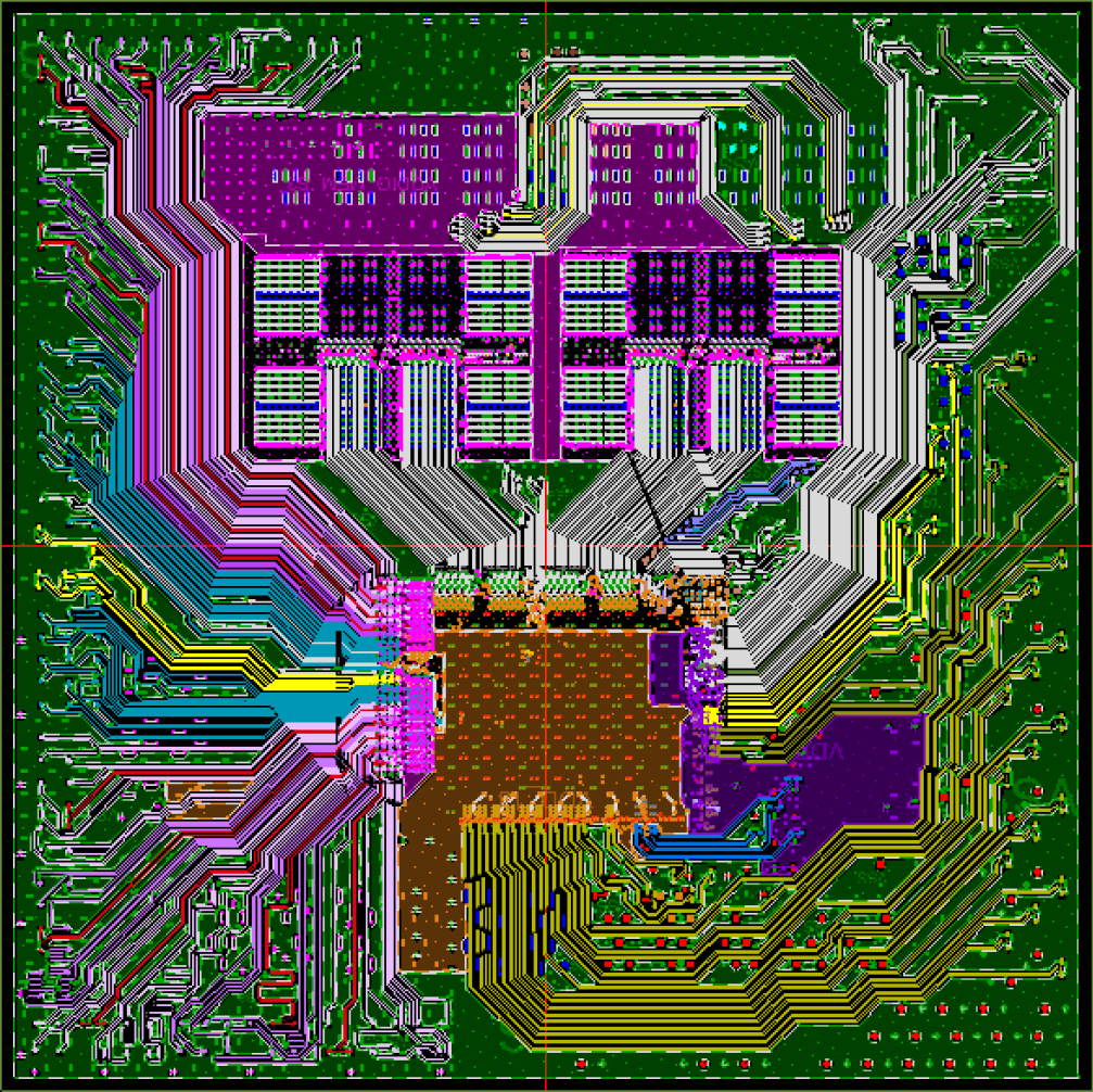
  • A 15 layer Telescoping Metal stack has been co-optimized to deliver both high frequency and high density routing capability
This bodes well for density going forward, since they managed to increase frequency greatly without adding additional metal layers. Probably RDNA3 will hit in the same range for density ~90MTr/mm2 and probably blazing frequency if thermal hotspots can be taken care of.
They did add a lot more transistor to support AVX512/increasing ROB/L2/uop cache/BTB.

I bet the second GMI burnt a lot of space albeit probably a necessary forward looking block.

Zen5 will be a reset and optimize the core again a la Zen 3

Will be updated if more specs will show up. This time I doubt AMD will be more open
 
Last edited:

DisEnchantment

Golden Member
Mar 3, 2017
1,607
5,800
136
How much density does eLVT cost? Couldn't find a figure. Besides, doesn't the graph say the 70% of the core is still the standard 5nm HD cells, with the specialized cells prob just being along the critical paths?
So I don't know if this means Zen 5 could claw back much density. Even if they go for no frequency gains or even a slight frequency drop, aren't wider architectures, which zen 5 will be, harder to clock higher as well?
What I intended to mean was the focus on significant frequency gain was causing a trade off in density.
Here is the answer to the significant frequency gains achieved ..... Also the reason for the significant loss of density.

eLVT caused higher leakage due to lower threshold (but faster switching) which increased energy usage.
N4P uses more EUV in the metal layers which improves cell density.
Finer metal layers, improved Cac, avoiding eLVT, no additional metal layers will make a difference in cell performance and energy efficiency with an opportunity to reduce cell dimension.

Even though Zen 5 could be wider, the excellent efficiency of N4P (+22% over N5, probably more over N5 w/ eLVT) should be able to reduce cell switching power requirement and can sustain same high frequency if not more.
 
Last edited:

Geddagod

Golden Member
Dec 28, 2021
1,157
1,020
106
What I intended to mean was the focus on significant frequency gain was causing a trade off in density.


eLVT caused higher leakage due to lower threshold (but faster switching) which increased energy usage.
N4P uses more EUV in the metal layers which improves cell density.
Finer metal layers, improved Cac, avoiding eLVT, no additional metal layers will make a difference in cell performance and energy efficiency with an opportunity to reduce cell dimension.

Even though Zen 5 could be wider, the excellent efficiency of N4P (+22% over N5, probably more over N5 w/ eLVT) should be able to reduce cell switching power requirement and can sustain same high frequency if not more.
Do we know if Zen 5 is going to use N4P?
And ye, I'm sure that N4P brings density improvements over N5, but it really isn't that much. It's like 6%.
And while the extra energy efficiency is nice, it's much harder to translate that into actual frequency. N4P brings a 11% frequency boost iso voltage, but that would most likely shrink at the extremely high clocks as well. The difference with this and e-LVT seems that e-LVT boosts the max frequency a good bit, while standard node shrinks are better at increasing frequency iso power along the entire curve, but that doesn't necessarily mean the same F-Max would benefit nearly as much. At least this is what it looks like to me.
So I still don't think they can squeeze that much extra density out of Zen 5. think CCX is going to stay the same on Zen 5 compared to Zen 4. In comparison, Zen 3 to Zen 2 it grew by 16%, but zen 3 also didn't have the sub node advantage Zen 5 will have. For 4nm Zen 5 atleast, idk about 3nm.
 
  • Like
Reactions: scineram

DisEnchantment

Golden Member
Mar 3, 2017
1,607
5,800
136
Do we know if Zen 5 is going to use N4P?
And ye, I'm sure that N4P brings density improvements over N5, but it really isn't that much. It's like 6%.
And while the extra energy efficiency is nice, it's much harder to translate that into actual frequency. N4P brings a 11% frequency boost iso voltage, but that would most likely shrink at the extremely high clocks as well. The difference with this and e-LVT seems that e-LVT boosts the max frequency a good bit, while standard node shrinks are better at increasing frequency iso power along the entire curve, but that doesn't necessarily mean the same F-Max would benefit nearly as much. At least this is what it looks like to me.
So I still don't think they can squeeze that much extra density out of Zen 5. think CCX is going to stay the same on Zen 5 compared to Zen 4. In comparison, Zen 3 to Zen 2 it grew by 16%, but zen 3 also didn't have the sub node advantage Zen 5 will have. For 4nm Zen 5 atleast, idk about 3nm.
We shall know next year not much is there to discuss at the moment.
 

Geddagod

Golden Member
Dec 28, 2021
1,157
1,020
106
1678081948453.png
In this AMD Zen 4 die shot, where are the Int Reg? Also in the die shot, is the part labelled scheduler just for INT since the unit labelled FP also has a FP scheduler (according to Locuza die shot)?
 

NostaSeronx

Diamond Member
Sep 18, 2011
3,686
1,221
136
View attachment 77704
In this AMD Zen 4 die shot, where are the Int Reg? Also in the die shot, is the part labelled scheduler just for INT since the unit labelled FP also has a FP scheduler (according to Locuza die shot)?
Int Registers should be in Int ALU polygon.

The scheduler part is mostly for the mid-core(integer core).

Scheduler (every to the first etc. stuff should be in the scheduler polygon):
Core Retire (Retire Queue / FPU Address Generation is solved in Integer)
Integer Rename (Integer Mapper)
Integer Schedulers (Integer Queues)
etc. stuff

FPU (everything below is the middle part of the FPU polygon):
FPU Retire (FPU's Retire queue is inside the FPU, and is significantly smaller than the Core Retire) <-- This is also considered NSQ, but it is actually the FPU ROB/Retire.
FPU Rename+ ("NSQ" { FPU Load/Store is done here) <-- NSQ is actually this part.
FPU Schedulers (FPU Queues)
etc. Stuff
 
Last edited:

Geddagod

Golden Member
Dec 28, 2021
1,157
1,020
106
Someone might want to check me on this, but is Zen 4's 512KB data array actually larger than Intel Redwood Cove's 512KB L2 data array? Based on the die shots it certainly looks like it.
 

DisEnchantment

Golden Member
Mar 3, 2017
1,607
5,800
136
Just came across this gem
Zen 4 CCX --> 55mm2 for 6.5B XTors, Zen 4 CCD --> 66.3mm2 for 6.57 B XTors

So SMU + DBG + IFOP is only 700 M XTors --> The IFOP really consumed a lot of space for not so much XTors used! On the other had, the CCX has an amazing density of 118 MTr/mm2, different picture when looking at CCD MTr/mm2 values
1679840954609.png
1679840974878.png

Learnt something new which I overlooked.
 
Last edited:

BorisTheBlade82

Senior member
May 1, 2020
664
1,014
106
Just came across this gem
Zen 4 CCX --> 55mm2 for 6.5B XTors, Zen 4 CCD --> 66.3mm2 for 6.57 B XTors

So SMU + DBG + IFOP is only 700 M XTors --> The IFOP really consumed a lot of space for not so much XTors used! On the other had, the CCX has an amazing density of 118 MTr/mm2, different picture when looking at CCD MTr/mm2 values
View attachment 78653
View attachment 78654

Learnt something new which I overlooked.
No, it is not 700.000.000 Xtors. It is just 70.000.000 o.0
 

DisEnchantment

Golden Member
Mar 3, 2017
1,607
5,800
136
There is a lot to be gained from switching the Interconnects from a die area savings perspective alone.
The GLink-2.5D IP utilizes single-ended signaling on parallel bus with DDR clock forwarding. This allows for up to 8/16Gbps per pin consuming only 0.25pJ/bit on TSMC’s RDL-based InFO (Integrated-Fan-Out) or CoWoS (Chip-on-Wafer-on-Substrate). One slice has 32 full-duplex lanes and one PHY has 8 slices with 2/4Tbps maximum bandwidth. For the next generation GLink, one slice will have 56 full-duplex lanes and one PHY has 8 slices with 7.5 Tbps maximum bandwidth.
GLink style interconnect is the way to go. 3mm beachfront for 2Tbps.
1679849640301.png
1679849487208.png
 

BorisTheBlade82

Senior member
May 1, 2020
664
1,014
106

GLink style interconnect is the way to go. 3mm beachfront for 2Tbps.
View attachment 78660
View attachment 78658
?
This is Terrabit/s/mm, right? So I would say 3mm per 1 TByte/s. Sounds like what we already have with N31 (silicon proven). But impressive nevertheless.
 

naukkis

Senior member
Jun 5, 2002
706
578
136
Not that surprising. IO doesn't really shrink since there's a minimal physical distance needed for pins/wires and you can't get around that no matter how small your transistors get.

Whole chip surface can be used for IO interface. IO logic doesn't shrink because physical off-chip data transfer needs current many magnitudes more than what is possible with smallest transistors. So IO needs to be done with quite a big logic transistors.
 

Mopetar

Diamond Member
Jan 31, 2011
7,837
5,992
136
I'm not quite sure what you mean by bigger transistors because the size doesn't matter. If you're moving some data off chip it has to be done over a physical interface which has a very specific design and a set of specifications under which it must operate. The size of the transistors don't matter because the limits are due to physical design of the bus and the protocol for data transferred across. Making that part smaller would change the performance or introduce errors that the other end isn't equipped to deal with.

The physical interface between the chip and the off-chip bus may eventually require larger components than could otherwise be fabricated, but the pin/wire size and similar requirements will always drive size requirements more than anything else. Even if you could drive the connection with smaller transistors it wouldn't matter because the space they would occupy doesn't go down. IO is always on the edge of the chip because it's easier to connect. The pins are part of the package, not the CPU itself.
 
  • Like
Reactions: BorisTheBlade82

Abwx

Lifer
Apr 2, 2011
10,951
3,469
136
I'm not quite sure what you mean by bigger transistors because the size doesn't matter. If you're moving some data off chip it has to be done over a physical interface which has a very specific design and a set of specifications under which it must operate. The size of the transistors don't matter because the limits are due to physical design of the bus and the protocol for data transferred across. Making that part smaller would change the performance or introduce errors that the other end isn't equipped to deal with.

The physical interface between the chip and the off-chip bus may eventually require larger components than could otherwise be fabricated, but the pin/wire size and similar requirements will always drive size requirements more than anything else. Even if you could drive the connection with smaller transistors it wouldn't matter because the space they would occupy doesn't go down. IO is always on the edge of the chip because it's easier to connect. The pins are part of the package, not the CPU itself.


Transistors s size does matter, the bigger the higher the current and power dissipation capabilities.

Old CPUs with much less but bigger xtors could be overclocked at comparable TDPs than more recent and transistors inflated ones..

IO need more drive currents than say a few transistors gates, hence higher currents will require either bigger transistors or paralleling several smaller transistors, wich amount to the same, that is , a lower density.
 

naukkis

Senior member
Jun 5, 2002
706
578
136
I'm not quite sure what you mean by bigger transistors because the size doesn't matter. If you're moving some data off chip it has to be done over a physical interface which has a very specific design and a set of specifications under which it must operate. The size of the transistors don't matter because the limits are due to physical design of the bus and the protocol for data transferred across. Making that part smaller would change the performance or introduce errors that the other end isn't equipped to deal with.

The physical interface between the chip and the off-chip bus may eventually require larger components than could otherwise be fabricated, but the pin/wire size and similar requirements will always drive size requirements more than anything else. Even if you could drive the connection with smaller transistors it wouldn't matter because the space they would occupy doesn't go down. IO is always on the edge of the chip because it's easier to connect. The pins are part of the package, not the CPU itself.

IO-pins does need physical output from silicon, but as those outputs are metal layers they can routed anywhere from silicon so overall silicon space matters how much IO can routed from chip. Like AMD showed their Zen2 package routing picture IO from Zen2 CCD is routed from L3-area of chip. IO-driving transistors instead need silicon space as they aren't just metal layers but half conductors which need their own part from silicon - and as those transistor chains have to drive physical interface those transistors need much bigger physical implementation than minimum size manufacturing process allows - IO part of logic won't scale much at all with manufacturing process, though they will scale to improved physical implementations.

Routing.png