-
We’re currently investigating an issue related to the forum theme and styling that is impacting page layout and visual formatting. The problem has been identified, and we are actively working on a resolution. There is no impact to user data or functionality, this is strictly a front-end display issue. We’ll post an update once the fix has been deployed. Thanks for your patience while we get this sorted.
You are using an out of date browser. It may not display this or other websites correctly.
You should upgrade or use an alternative browser.
You should upgrade or use an alternative browser.
Question Which Process node does SD 7g1 use ?
- Thread starter FlameTail
- Start date
Tech Junky
Diamond Member
I don't know about this specifically but QCOM switched to TSMC after some issues on SD8G1 and produced SD8G1+ with some decent improvements and will be using TSMC moving forward for SD8G2 due to the better performance on their fabs vs SS. The overheating issues with G1 went away with G1+ on TSMC.
If you want to see more specs figure out the model number of the SD7G1 and then plug it into news.google.com and tons of reviews and insights should come up and answer your question.
If you want to see more specs figure out the model number of the SD7G1 and then plug it into news.google.com and tons of reviews and insights should come up and answer your question.
Last edited:
FlameTail
Diamond Member
If you mean Snapdragon 8 gen 1, that's Samsung 4LPE.
Snapdragon 8 gen 1 is made in 4LPX.
DrMrLordX
Lifer
Snapdragon 8 gen 1 is made in 4LPX.
Based on what?
Gen 1 and Exynos 2200 should both be 4LPE. I've seen a few sources claim otherwise, that the 2200 was 4LPE while the 8 Gen 1 is 4LPX, but I don't see why Qualcomm would have initially used an LPX node for mobile until it became obvious that N4 was just that much better (see: Dimensity 9000).
This blog claims that 8+ Gen 1 is dual-sourced on N4 and 4LPX:
Qualcomm Snapdragon 8(+) Gen1 SoC | TechInsights
For the first time in recent memory, Qualcomm has dual-sourced their Snapdragon 8(+) Gen1 SoC with both Samsung (4LPX) and TSMC (N4). This has allowed us at TechInsights to compare a common design manufactured by two different foundries.
(which is also weird)
FlameTail
Diamond Member
Qualcomm Snapdragon 8(+) Gen1 SoC | TechInsights
For the first time in recent memory, Qualcomm has dual-sourced their Snapdragon 8(+) Gen1 SoC with both Samsung (4LPX) and TSMC (N4). This has allowed us at TechInsights to compare a common design manufactured by two different foundries.
That's absurd. If they are dual-sourced, that doesn't explain how the Sd 8(+) gen1 has better efficiency and performance than the Sd 8 gen1.
If it is dual sourced, their would certainly be a performance disparity between the Samsung manufactured one and TSMC manufactured one, and so far the reviewers have found none.
FWIW, Qualcomm themselves stated that the SD 8+ G1 is made on TSMC node. The entire value proposition of the Sd 8+ g1 is the fact that it is made on the TSMC node, which is what almost every other media outlet has been reporting.
FlameTail
Diamond Member
Wikipedia is the last website I would trust for minute details like this. Every other site i have seen so far has stated that SD 8g1 is made on Samsung 4LPX, whereas Exynos 2200 is made on 4LPE.
Indeed this can be logically explained by the fact that 4LPX is a more performance-oriented node while 4LPE is a more efficient node. In benchmarks the SD 8g1 surpasses the Exynos 2200 in performance, which can be explained by the node difference.
FlameTail
Diamond Member
Qualcomm Snapdragon 8(+) Gen1 SoC | TechInsights
For the first time in recent memory, Qualcomm has dual-sourced their Snapdragon 8(+) Gen1 SoC with both Samsung (4LPX) and TSMC (N4). This has allowed us at TechInsights to compare a common design manufactured by two different foundries.www.techinsights.com
That's absurd. If they are dual-sourced, that doesn't explain how the Sd 8(+) gen1 has better efficiency and performance than the Sd 8 gen1.
If it is dual sourced, their would certainly be a performance disparity between the Samsung manufactured one and TSMC manufactured one, and so far the reviewers have found none.
FWIW, Qualcomm themselves stated that the SD 8+ G1 is made on TSMC node. The entire value proposition of the Sd 8+ g1 is the fact that it is made on the TSMC node, which is what almost every other media outlet has been reporting.
Edit: And, ironically the said wikipedia article you quoted itself says that the SD 8+ g1 is made on TSMC N4, and there is no mention of dual sourcing. >_<
DrMrLordX
Lifer
Edit: And, ironically the said wikipedia article you quoted itself says that the SD 8+ g1 is made on TSMC N4, and there is no mention of dual sourcing. >_<
Two different sources saying two different things.
I think it can honestly be said that there is very little agreement on where, or if, 4LPX was used in Qualcomm's products.
It is most likely that the 8 Gen 1 is 4LPE since generally Samsung uses the LPE nodes for mobile products. It's possible that they have some 8+ Gen 1 chips on 4LPX sold in particular markets, which might explain why predominantly English-speaking reviewers didn't get their hands on any phones using those chips. That's assuming dual-sourcing happened at all.
Here is another source claiming that the 8 Gen 1 is 4LPE:
Dimensity 9000 vs Snapdragon 8 Gen 1 | Which chipsets Is Better? - Xiaomiui.Net
In this article, we will compare in detail the 2 chipsets, Dimensity 9000 vs Snapdragon 8 Gen 1, which were introduced towards the end of 2021. 2021 year
 xiaomiui.net
Last edited:
FlameTail
Diamond Member
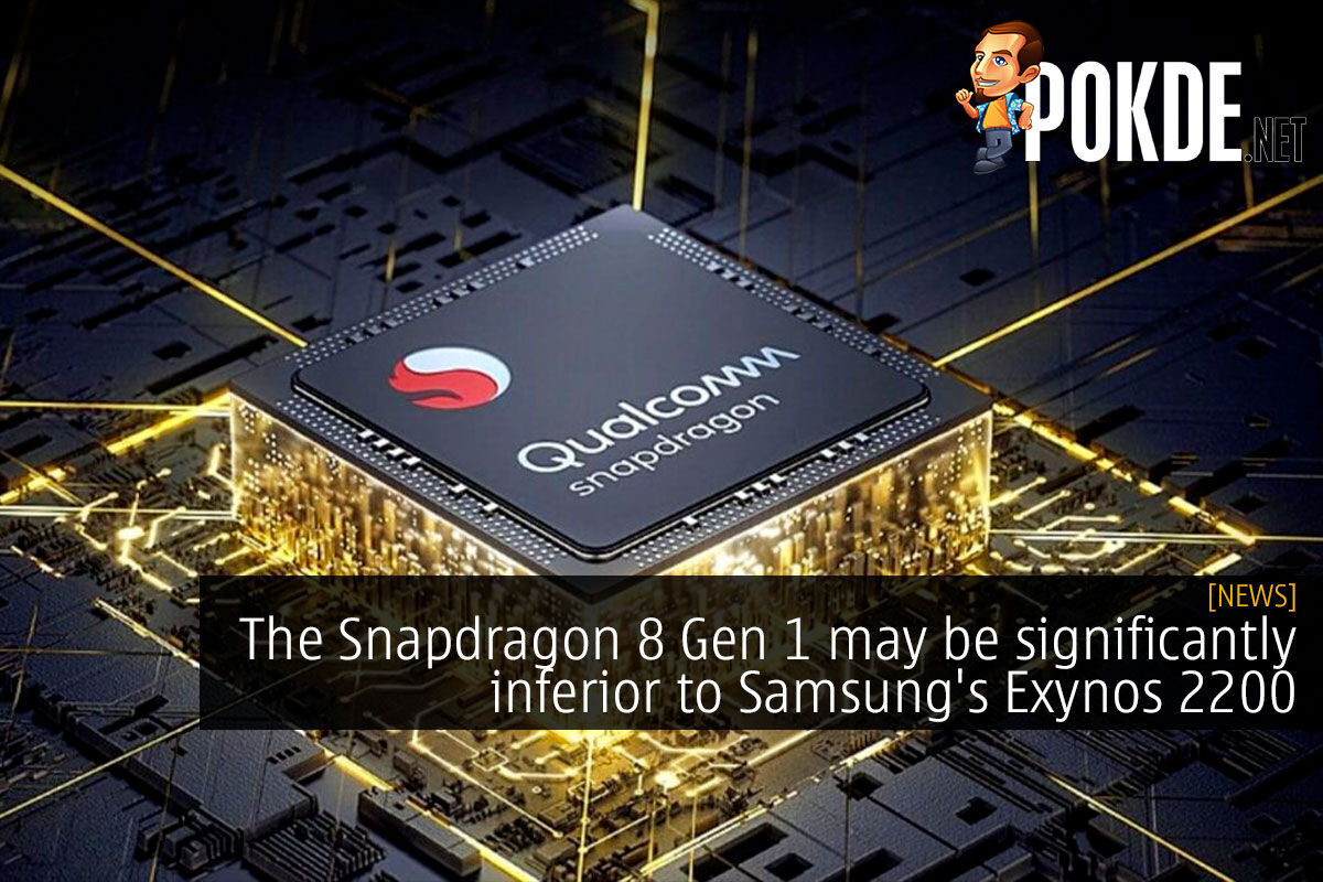
The Snapdragon 8 Gen 1 May Be Significantly Inferior To Samsung's Exynos 2200 – Pokde.Net
Rumors are cropping up that the Snapdragon 8 Gen 1 (or Snapdragon 898) may be significantly worse than the Exynos 2200.
 pokde.net
This article explains the difference between 4LPX and 4LPE. Essentially, 4LPX is a rebranded 5LPP node. On the other hand, 4LPE is a new ground up node.
This image comes from Samsung themselves and shows the positioning of their various nodes. Incidentally, it fits with what the article I quoted says, in that Samsung 4nm is a new ground up node and Samsung 5nm family sits under the 7LPP family.
Overheating issues didnt go away, its just Oem figure out how to throttle these soc. Without throttling sd 8+ Gen 1 phones overheat to the point its uncomfortable to touch.I don't know about this specifically but QCOM switched to TSMC after some issues on SD8G1 and produced SD8G1+ with some decent improvements and will be using TSMC moving forward for SD8G2 due to the better performance on their fabs vs SS. The overheating issues with G1 went away with G1+ on TSMC.
If you want to see more specs figure out the model number of the SD7G1 and then plug it into news.google.com and tons of reviews and insights should come up and answer your question.
That would happen to any processor inside anything without dissipation.Overheating issues didnt go away, its just Oem figure out how to throttle these soc. Without throttling sd 8+ Gen 1 phones overheat to the point its uncomfortable to touch.
The SD8+1 is indeed noticeably more efficient.
Its is more efficient than 8G1 but still use way more power than average smartphone soc.That would happen to any processor inside anything without dissipation.
The SD8+1 is indeed noticeably more efficient.
That X2 core alone use 4 to 4.5W
TRENDING THREADS
-
 Discussion Zen 5 Speculation (EPYC Turin and Strix Point/Granite Ridge - Ryzen 9000)
- Started by DisEnchantment
- Replies: 25K
-
Discussion Intel Meteor, Arrow, Lunar & Panther Lakes + WCL Discussion Threads
- Started by Tigerick
- Replies: 25K
-
 Discussion Intel current and future Lakes & Rapids thread
- Started by TheF34RChannel
- Replies: 24K
-

-
