What should the TDP of the next optimized for mobile AMD APU be?

Page 3 - Seeking answers? Join the AnandTech community: where nearly half-a-million members share solutions and discuss the latest tech.

What should the TDP of the next optimized for mobile AMD APU be?

  • 35W to 45W is fine

    Votes: 25 78.1%
  • 55W to 70W

    Votes: 2 6.3%
  • 75W to 90W

    Votes: 0 0.0%
  • 95W to 110W

    Votes: 0 0.0%
  • 115W or greater

    Votes: 1 3.1%
  • 135W to 150W

    Votes: 1 3.1%
  • Greater than 155W (Whatever)

    Votes: 3 9.4%

  • Total voters
    32

cbn

Lifer
Mar 27, 2009
12,968
221
106
Another reference point to take a look at:

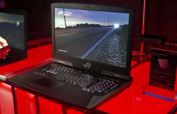
Asus ROG Strix GL702ZC (This is a 17.3" 7.04 lb laptop with a 65W Ryzen AM4 CPU (using B350 chipset) and a mobile RX580 4GB* in it)

https://www.bit-tech.net/previews/t...preview-asus-rog-strix-gl702zc-benchmarked/1/

We didn’t have time to do a full tear-down, but hidden beneath the cooler is the six-core Ryzen 5 1600 CPU sporting its usual six cores. It carries all the same specs as the desktop part including 3.2GHz / 3.6GHz base and boost clocks. The TDP of this chip is a hefty 65W. The other component directly cooled is, of course, the Radeon RX 580 GPU and associated 4GB of GDDR5. The core is clocked at 1,077MHz, which is down from the 1,340MHz boost clock of the desktop part, but the memory is at the same 8Gbps as the desktop model.

(NOTE: Ryzen 7 1700 is also available)

*Notebookcheck estimates the power consumption of the mobile RX580 to be around 89W.....so the 65W CPU and dGPU together would consume 154W.

Meanwhile, the Radeon RX 580 should be around 90% the performance of an Nvidia GTX 1060, but will consume 10-11% more power.

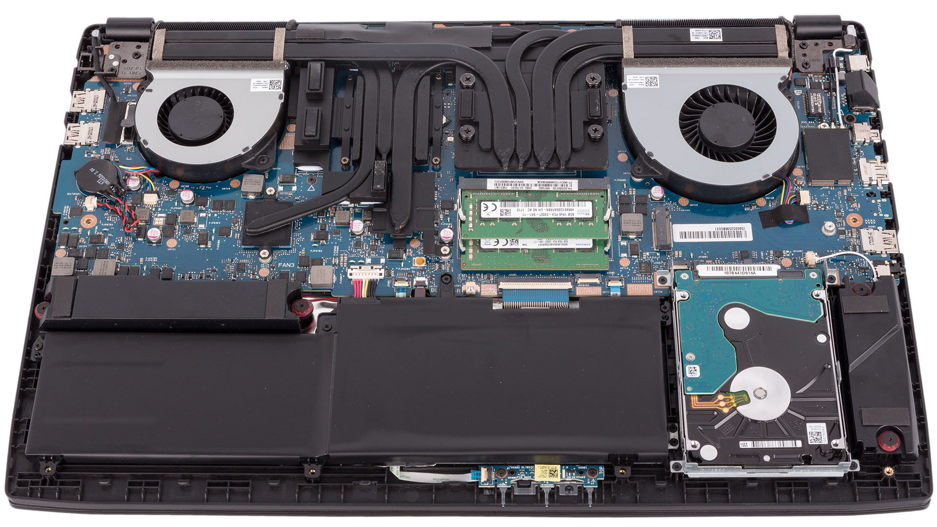
Here is what the cooling looks like:
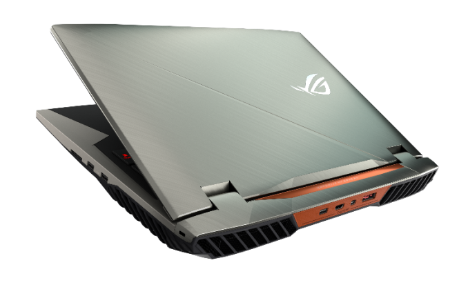
39bdbb14-f0ae-4017-9bcf-6b8402ba6aed.jpg
 

scannall

Golden Member
Jan 1, 2012
1,946
1,638
136
For mobile, the biggest part of the market is in the 15 to 30 watt range. I'm guessing that's where they will spend the most time and money aiming.
 

ao_ika_red

Golden Member
Aug 11, 2016
1,679
715
136
For mobile, the biggest part of the market is in the 15 to 30 watt range. I'm guessing that's where they will spend the most time and money aiming.
5-35w segment to be precise. But, by battling in crowded market means a razor-thin margin per item. OP seems to prefer hi-perf/gaming/power laptops because that's where the lucrative profit should be.
 

cfenton

Senior member
Jul 27, 2015
277
99
101
^^^^ Another thing to consider (besides packaging size) is capability.

Example: For a content creation laptop (eg, Video editing and 3D Creation) having up to 16C/32T (rather than up to 8C/16T) would be a very nice for the APU. This for either a 15.6" or 17.3" laptop.

P.S. 17.3" laptops with relatively high TDP (GTX 1070) can be fairly light as shown by the following models (two of which are under 6 lbs while the rest are under 7 lbs)---> https://www.newegg.com/Product/ProductList.aspx?Submit=ENE&N=100167748 601206491 8000 4814 601206490 600553910 600004928 600004929&IsNodeId=1&bop=And&Order=PRICE&PageSize=36 .

I've never seen a design that uses one big fan, rather than two smaller fans. I suppose it could be done, but cooling 125W would require quite the heatsink and fan combo.

I wouldn't consider 6 lbs to be light, really. It's better than some of the absurd gaming laptops that weigh 15 lbs, but it still wouldn't be fun to carry around all day. I have a 4 lbs laptop at the moment, and even that feels heavy compared to some of the ultrabooks my friends have. I know weight isn't important for everyone, but it is to me.
 

cbn

Lifer
Mar 27, 2009
12,968
221
106
For mobile, the biggest part of the market is in the 15 to 30 watt range. I'm guessing that's where they will spend the most time and money aiming.

Yes, 35W APUs like Raven Ridge that can configured in a range of TDPs from low to high are very important.

But I think there is a lot of room for improvement in the very high watt laptop category (currently served by CPU and dGPU).... and have been wondering if AMD will serve this area (in addition to the 35W) by adapting Zen HPC Server APUs.

However, now that I have looked into this further I have to wonder if the high watt laptops would come first then the HPC Servers?
 
Last edited:

ao_ika_red

Golden Member
Aug 11, 2016
1,679
715
136
Ah, got it. That's why you're very insisted on 100W+ APU. Based on how Vega currently unfolded, I doubt a big APU will land on consumer laptops soon.
1. Big die such as Vega currently has poor yield.
2. It needs vast amount of bandwidth to fuction properly. It won't work with current DDR4 and because HBM2 also yields poorly and makes it more problematic to use.
3. AMD APU history tells us that it aimed mainly to mainstream market (200-700 dollar). And I don't think huge APU will make it to that market.

I don't think we'll see a high power APU in near future. But, once Global Foundries 7nm process is mature enough, current rumour about 6C/CCX of Zen2, modularity promised by Navi, and next gen memory that comes with Navi, I expect a big APU in 2020 onwards.
 
Last edited:

LightningZ71

Golden Member
Mar 10, 2017
1,627
1,898
136
Just thinking out loud...
Perhaps a mobile workstation APU?
Model it after the threadripper MCM.
One chip is a binned mobile ryzen 8 core chip, the other is a Vega chip. 4 channels of DDR4. Only one module to cool.
 
  • Like
Reactions: cbn

cbn

Lifer
Mar 27, 2009
12,968
221
106
Just thinking out loud...
Perhaps a mobile workstation APU?
Model it after the threadripper MCM.
One chip is a binned mobile ryzen 8 core chip, the other is a Vega chip. 4 channels of DDR4. Only one module to cool.

That is very similar to a HPC APU design rumored back in in 2015. (The main difference is that you are mentioning one CPU die rather than the two needed for quad channel memory)

P.S. Here is some info from the following AMD 2017 Research Paper (which looks farther into the future of HPC APUs) --> http://www.computermachines.org/joe/publications/pdfs/hpca2017_exascale_apu.pdf

AMD.EHP_.png


2) Modular Chiplet Design: The performance requirements of the exascale node require a large amount of compute and memory to be integrated into a single package. Rather than build a single, monolithic system on chip (SOC), we propose to leverage advanced die-stacking technologies to decompose the EHP into smaller components consisting of active interposers and chiplets. Each chiplet houses either multiple GPU compute units or CPU cores. The chiplet approach differs from conventional multi-chip module (MCM) designs in that each individual chiplet is not a complete SOC. For example, the CPU chiplet contains CPU cores and caches, but lacks memory interfaces and external I/O.1 There are multiple benefits to this decompositional approach to SOC construction: Die Yield: Building a single monolithic SOC that provides the equivalent capabilities of what we propose for the EHP would result in an impractically large chip with prohibitive costs. Smaller chiplets have higher yield rates due to their size, and when combined with known-good-die (KGD) testing techniques, can be assembled into larger systems at reasonable cost. This approach has already started garnering interest in both academia [9] and industry [8], [19]. Process Optimization: A monolithic SOC imposes a single process technology choice on all components in the system. With chiplets and interposers, each discrete piece of silicon can be optimized for its own functions. For example, the CPU chiplets can use performance-optimized devices and metal layers, while the GPU chiplets use density-optimized devices and metal. The interposer layers can use a more mature (i.e., less expensive) process technology node as the I/O components likely do not need transistors in the cuttingedge technology node nor as many metal routing layers as the compute chiplets. Re-usability: A single, large HPC-optimized APU would be great for HPC markets, but may be less appropriate for others. The decomposition of the EHP into smaller pieces enables silicon-level reuse. For example, one or more of the CPU clusters could be packaged together to create a conventional CPU-only server processor.

3) Active Interposers: There are several options for the assembly of multiple discrete pieces of silicon within the same package. For example, MCMs have been used for years, and they have even been proposed in the context of chiplets as advocated by Marvell’s MoChi (Modular Chips) concept [8]. Passive silicon interposers are also already in volume production, in particular for the integration of GPU and 3D memory as demonstrated by AMD’s RadeonTM R9 Fury GPU [20]. However, due to the sheer amount of compute, memory, and other logic that we aim to integrate into the EHP package, we found true 3D stacking on top of active interposers to be desirable. Active interposers are fundamentally no different than other 3D stacking approaches considered by past research2 , and preliminary prototypes have even been successfully constructed and demonstrated [21]. Contrast this to typical MCM parts that take identical CPU chips that are each fully functional SOCs, and then place them in the same package. With chiplets, there is no option to take a single chiplet by itself and convert it into a complete product without additional silicon.
 
Last edited:

LightningZ71

Golden Member
Mar 10, 2017
1,627
1,898
136
That's roughly what I was imagining, though, more next generation. I was thinking more in the line of something that's doable with today's available components. Using an actual Ryzen chip, and a Vega chip on a traditional MCM, connected to each other via IF on the MCM, with the Ryzen having two channels of DDR4 attached to it, and the VEGA having its own memory controller either running GDDR5, traditional DDR4, or, on a higher end product, an HBM stack on the MCM. The integrated MCM stack would serve to keep pinout down, but would add its own significant heat source to the MCM, which will already be difficult to keep thermally managed. This could make for quite a high performance laptop, that is still reasonable to cool, without requiring the large footprint of existing gaming laptops, and likely also a reduced mass as well. Just look up thread at the gaming laptop displayed there. Half of those heat pipes could be eliminated with the CPU and GPU shared a MCM. Granted, the remaining ones would need to be thicker, but the total area consumed would be reduced, allowing for potentially larger, slower, quieter fans and larger radiators.

And, no, I don't expect that it will compete with the top end of the dGPU gaming laptops, but I expect it to be a solid choice for 1080p laptop gaming and to be able to drive a decent external display, even at 4K but with reduced graphics quality.
 
  • Like
Reactions: cbn

NTMBK

Lifer
Nov 14, 2011
10,230
5,007
136
Here is a telescoping controller that works with up to 10" Windows (and Android/iOS) tablets:

http://www.ipega.hk/index.php?option=com_phocagallery&view=detail&catid=11:iphone&id=1100:bluetooth-stretch-controller&Itemid=4&lang=en

https://www.amazon.com/IPEGA-Telescopic-Wireless-Bluetooth-Controller/dp/B00RE6FMD8


(Note the tablet used in the above video is a Dell Venue 11 with a 10.8" 1080p screen)


51RUsox9YNL._SL1024_.jpg


So NTMBK, Is a 12W Raven Ridge in detachable tablet-laptop with a 10.8" screen workable?

Yes, it will mostly be running very low clocks (when used as a gaming device).....but perhaps it will be faster than I originally thought--> https://gfxbench.com/compare.jsp?benchmark=gfx40&did1=53156431&os1=Windows&api1=gl&hwtype1=iGPU&hwname1=AMD+Radeon(TM)+Vega+10+Mobile+Graphics&D2=AMD+A12-9800E+RADEON+R7,+12+COMPUTE+CORES+4C+8G )

Believe it or not, I have actually tried that- with that same controller, and with a Venue 11! It's pretty awful. I was using the Venue 11 7130, and it's just too big and heavy to be comfortable- especially since the controller only supports the bottom of the tablet. I think 7-8" is the realistic limit to what you can do in a handheld.

12W is just too much to cram into a handheld. The whole device gets warm, the fan is whining away, and it's not a comfortable experience.

EDIT: The Linx Vision is a better example- 8" tablet with XBox controller dock.

135473-tablets-news-best-windows-10-tablet-for-playing-xbox-one-the-linx-vision-is-a-bargain-at-149-image1-oBas8tSV7e.jpg


http://www.linxvision.co.uk/
 

cbn

Lifer
Mar 27, 2009
12,968
221
106
I personally prefer 20W max. Anything higher either means high noise levels or increase in the system size and weight.

What screen size for the 20W?

Also how much does increasing screen size to 17.3" affect this number of 20W?
 

cbn

Lifer
Mar 27, 2009
12,968
221
106
What should the TDP of the next optimized for mobile AMD APU be?
  1. 35W to 45W is fine
    23 vote(s)
    79.3%
  2. 55W to 70W
    1 vote(s)
    3.4%
  3. 75W to 90W
    0 vote(s)
    0.0%
  4. 95W to 110W
    0 vote(s)
    0.0%
  5. 115W or greater
    1 vote(s)
    3.4%
  6. 135W to 150W
    1 vote(s)
    3.4%
  7. Greater than 155W (Whatever)
    3 vote(s)
    10.3%

Very surprised to see so few votes for a 55W or greater mobile optimized TDP.

I wonder how many people voted this way because Intel has the Radeon equipped Kabylake-G at the 65W and 100W level?
 
Last edited:

NTMBK

Lifer
Nov 14, 2011
10,230
5,007
136
Very surprised to see so few votes for a 55W or greater mobile optimized TDP.

I wonder how many people voted this way because Intel has the Radeon equipped Kabylake-G at the 65W and 100W level?

I don't think that's a real thing. I think WCCFtech made it up.
 

cbn

Lifer
Mar 27, 2009
12,968
221
106
NTMBK,

I'll bet that chip is using Vega 11.
 
Last edited:

cbn

Lifer
Mar 27, 2009
12,968
221
106
Perhaps a mobile workstation APU?

I think that is a great usage.

........with ECC enabled (for the HBM2) it would be able to be used in ways Kabylake-G can't be whether APU has Vega 10 or Vega 11* GPU on board.

*Vega 11 not confirmed yet to have HBM2.
 
Last edited:

cbn

Lifer
Mar 27, 2009
12,968
221
106
Vega 20?

https://videocardz.com/65521/amd-vega-10-and-vega-20-slides-revealed

7nm, 4 stacks of HBM2, 1/2 rate FP64, ECC in 2H 2018

If true then this would the first high performance AMD GPU to have 1/2 rate FP64 since Hawaii/Grenada.

.....And something useful for workstation tasks relying heavily on FP64 (Simulations, etc.)

P.S. Was very happy to see AMD sponsor "Usage of Blender in Computer Aided Engineering (CAE)" at Blender Conference 2016 (Open Foam, of course, uses FP64....and can use the AMD GPU via the SpeedIT plugin). Perhaps in a few years this capability will be fully integrated into Blender?


EDIT: Fixed broken Youtube link.
 
Last edited:

cbn

Lifer
Mar 27, 2009
12,968
221
106
Something else to think about....

Bristol Ridge APU was unusual in that had 1/2 rate DP, but lacked memory bandwidth.

Could it be that AMD included the rumored HBM2 option for Raven Ridge in order to make 1/2 rate DP* work well enough that the APU could be used in HPC?

If so then I wonder about the possibility AMD could also release a 35W (or 45W) Raven Ridge APU with 1/2 rate DP, HBM2 (with ECC) for a (relatively lower power) workstation laptop focused on FP64 engineering tasks?

*I have no idea whether Raven Ridge has 1/2 rate DP or not. I am just speculating that the purpose of HBM2 was to support it.

P.S. Nvidia has a (big) Workstation card for FP64 engineering tasks called Quadro GP100 (uses GP100, 3584sp, 1/2 rate DP, 235W, 4096 bit HBM2). This, in comparison, to the higher TDP and higher stream processor (but much lower memory bandwidth) Quadro P6000 (uses GP102, 3840sp, 1/32 rate DP, 250W, 384 bit GDDR5) aimed mainly at FP32 engineering tasks.
 
Last edited:

cbn

Lifer
Mar 27, 2009
12,968
221
106
Just thinking out loud...
Perhaps a mobile workstation APU?
Model it after the threadripper MCM.
One chip is a binned mobile ryzen 8 core chip, the other is a Vega chip. 4 channels of DDR4. Only one module to cool.

That is very similar to a HPC APU design rumored back in in 2015. (The main difference is that you are mentioning one CPU die rather than the two needed for quad channel memory)

P.S. Here is some info from the following AMD 2017 Research Paper (which looks farther into the future of HPC APUs) --> http://www.computermachines.org/joe/publications/pdfs/hpca2017_exascale_apu.pdf

AMD.EHP_.png

Looking through that Paper I noticed AMD wants to supplement the estimated 256 GB of on die HBM-type memory (per node) with off package Hybrid Memory cubes (which use DRAM) as well as (in some cases) Non-volatile memory devices:

2) External-memory Network: The exascale target for per-node memory capacity is at least 1TB, which exceeds our in-package projections by a factor of four. As such, the ENA must augment the in-package memory with additional external memory. The ENA makes use of Memory Networks that consist of multiple memory modules interconnected with point-to-point links (as opposed to bus-based topologies for DDR) [29], [30]. A current example of this kind of memory approach is the Hybrid Memory Cube, which uses 3D-stacked DRAM inside each module, and the modules communicate with high-speed serial interfaces [31]

Depending on the exact needs of the supercomputer customer, the external-memory network could consist of a mix of both DRAM and non-volatile memory (NVM) devices. NVM provides higher densities and therefore could be useful in scenarios where very large problem sizes are important, or they could be used to reduce the total ENA board-level component count by meeting a given capacity target with fewer higher-capacity packages. The trade-off is that the NVMs are typically slower, consume more dynamic power (especially for writes), and may suffer from write endurance issues that could impact the system’s MTTF.

Seems like a good application for Hybrid Memory Cube with 3DXpoint rather than DRAM.
 
Last edited: