- Sep 11, 2014
- 1,484
- 5,088
- 136
Dont know if this have been posted in this forum yet, but here is a copy from wccftech.
Intel’s Lake Crest Chip Aims At The DNN/AI Sector – 32 GB HBM2, 1 TB/s Bandwidth, 8 Tb/s Access Speeds, More Raw Power Than Modern GPUs

Intel has further detailed their Lake Crest chip that will be aiming at the deep neural network sector. The new chip will be based around the Nervana platform which would deliver an unprecedented amount of compute density in silicon that delivers more raw power than modern GPUs.
Intel’s Lake Crest DNN Silicon Detailed – Will Feature More Raw Power Than GPUs
With the rise of AI learning in the tech industry, GPU makers such as NVIDIA and AMD have made chips that are specifically designed for DNN (Deep Neural Network) workloads. Intel wants to enter this ground with the Lake Crest silicon which is said to deliver more raw power than the fastest DNN GPUs available today. The chip will feature technology developed by the deep-learning startup, Nervana.

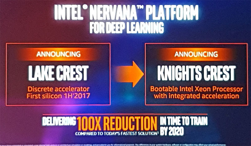
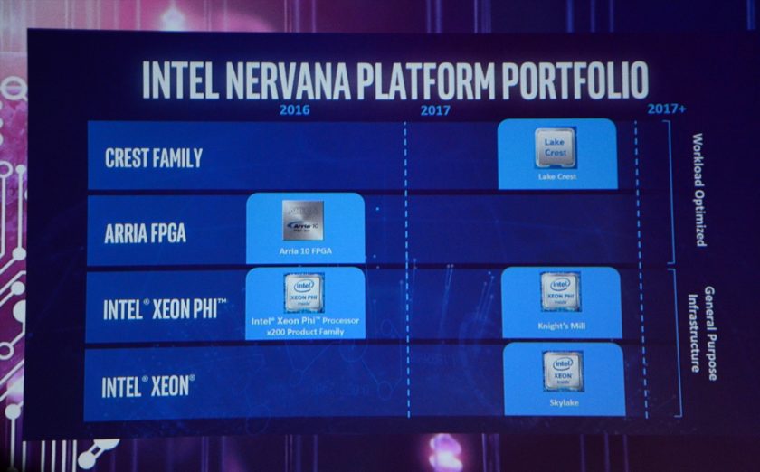
The software/hardware firm was acquired by Intel in August 2016 for more than $350 Million US. The first chip and systems to utilize the new Nervana based technology would be known as Lake Crest and Intel also named the follow up as “Knights Crest”. The Nervana platform which consists of an entire range of deep learning (DL) optimized products which would include Lake Crest and the recently announced ARRIA FPGAs which can also be programmed for special requirements and tasks such as AI learning. Both Lake Crest and ARRIA FPGAs will be working together with Intel’s Xeon processors.
Intel Lake Crest Chips Will Feature Unprecedented Amount of Compute Density, 32 GB of HBM2 Memory and 8 Terabits per Second Memory Access Speeds
The Lake Crest chip will operate as a Xeon Co-processor but is entirely different to the Xeon Phi hardware. It is specifically designed to boost AI workloads at an unprecedented pace. Intel is using a new architecture to be known as “Flexpoint” which will be used inside the arithmetic nodes of the Lake Crest chip. This will increase the parallelism of arithmetic operations for the chip by a factor of 10. The chip will also feature a MCM (Multi Chip Module) design.
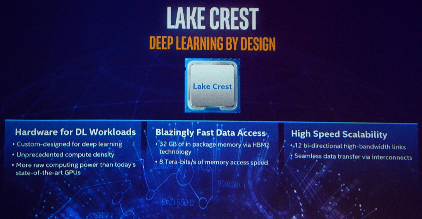
The discrete co-processor will feature a total of 32 GB of HBM2 memory. This will come in the form of four 8-Hi stacks which will deliver a total of 1 TB/s memory speeds at the rated clock speeds of 2 GHz. The Lake Crest chips will be available for testing during first half of 2017 and will be sampled to limited partners in the second half of 2017. Also to note is that the memory access speeds are rated at a whooping 8 Terabits per second.
Intel has also revealed that the chip will be highly scalable which is something their CEO, Brian Krzanich, has already stated to be the path forward for AI learning. The chip will feature 12 bidirectional high-bandwidth links and seamless data transfer via the interconnects. These proprietary inter-chip links will provide bandwidth up to 20 times faster than PCI Express links.
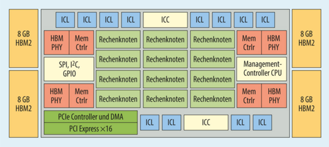
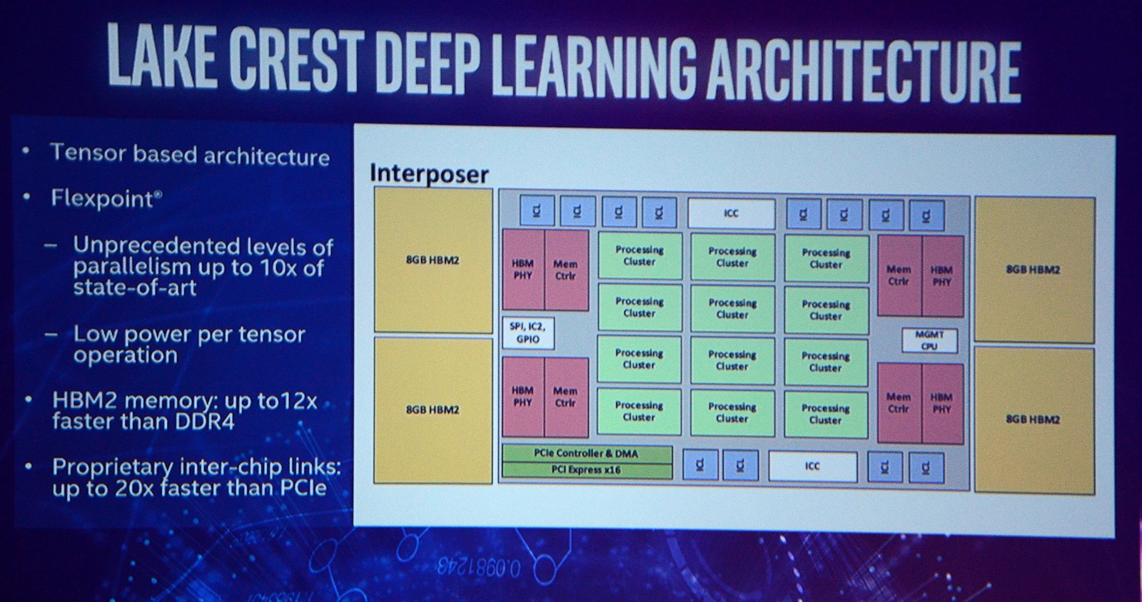
A detailed Lake Crest block diagram has been posted by Golem.de which shows the chip in more detail. We can see four 8 GB HBM2 memory blocks that are separate from the main die but will be featured on the same chip interposer. The chip contains 12 processing clusters which will feature several cores. Exact number has not yet been determined. Each HBM2 memory has its own HBM controller so there are four in total. There are 12 ICL (Inter-chip links) blocks for each processing cluster. There’s also a CPU management controller, SPI, IC2, GIPO, PCIe controller (x16) and DMA.
http://wccftech.com/intel-lake-crest-chip-detailed-32-gb-hbm2-1-tb/
Intel’s Lake Crest Chip Aims At The DNN/AI Sector – 32 GB HBM2, 1 TB/s Bandwidth, 8 Tb/s Access Speeds, More Raw Power Than Modern GPUs
Intel has further detailed their Lake Crest chip that will be aiming at the deep neural network sector. The new chip will be based around the Nervana platform which would deliver an unprecedented amount of compute density in silicon that delivers more raw power than modern GPUs.
Intel’s Lake Crest DNN Silicon Detailed – Will Feature More Raw Power Than GPUs
With the rise of AI learning in the tech industry, GPU makers such as NVIDIA and AMD have made chips that are specifically designed for DNN (Deep Neural Network) workloads. Intel wants to enter this ground with the Lake Crest silicon which is said to deliver more raw power than the fastest DNN GPUs available today. The chip will feature technology developed by the deep-learning startup, Nervana.
“We have developed the Nervana hardware especially with regard to deep learning workloads,” said Rao (Intel VP Datacenter Group and General Manager for AI solutions).”In this area, two operations are often used: matrix multiplication and convolution.” via Silicon.De
The software/hardware firm was acquired by Intel in August 2016 for more than $350 Million US. The first chip and systems to utilize the new Nervana based technology would be known as Lake Crest and Intel also named the follow up as “Knights Crest”. The Nervana platform which consists of an entire range of deep learning (DL) optimized products which would include Lake Crest and the recently announced ARRIA FPGAs which can also be programmed for special requirements and tasks such as AI learning. Both Lake Crest and ARRIA FPGAs will be working together with Intel’s Xeon processors.
Intel Lake Crest Chips Will Feature Unprecedented Amount of Compute Density, 32 GB of HBM2 Memory and 8 Terabits per Second Memory Access Speeds
The Lake Crest chip will operate as a Xeon Co-processor but is entirely different to the Xeon Phi hardware. It is specifically designed to boost AI workloads at an unprecedented pace. Intel is using a new architecture to be known as “Flexpoint” which will be used inside the arithmetic nodes of the Lake Crest chip. This will increase the parallelism of arithmetic operations for the chip by a factor of 10. The chip will also feature a MCM (Multi Chip Module) design.
AI is still in its early days, Krzanich writes, and the underlying hardware that’s used to execute deep learning tasks is bound to change. “Some scientists have used GPGPUs [general purpose graphical processing units] because they happen to have parallel processing units for graphics, which are opportunistically applied to deep learning,” he writes. “However, GPGPU architecture is not uniquely advantageous for AI, and as AI continues to evolve, both deep learning and machine learning will need highly scalable architectures.” via HPC Wire
The discrete co-processor will feature a total of 32 GB of HBM2 memory. This will come in the form of four 8-Hi stacks which will deliver a total of 1 TB/s memory speeds at the rated clock speeds of 2 GHz. The Lake Crest chips will be available for testing during first half of 2017 and will be sampled to limited partners in the second half of 2017. Also to note is that the memory access speeds are rated at a whooping 8 Terabits per second.
Intel has also revealed that the chip will be highly scalable which is something their CEO, Brian Krzanich, has already stated to be the path forward for AI learning. The chip will feature 12 bidirectional high-bandwidth links and seamless data transfer via the interconnects. These proprietary inter-chip links will provide bandwidth up to 20 times faster than PCI Express links.
A detailed Lake Crest block diagram has been posted by Golem.de which shows the chip in more detail. We can see four 8 GB HBM2 memory blocks that are separate from the main die but will be featured on the same chip interposer. The chip contains 12 processing clusters which will feature several cores. Exact number has not yet been determined. Each HBM2 memory has its own HBM controller so there are four in total. There are 12 ICL (Inter-chip links) blocks for each processing cluster. There’s also a CPU management controller, SPI, IC2, GIPO, PCIe controller (x16) and DMA.
http://wccftech.com/intel-lake-crest-chip-detailed-32-gb-hbm2-1-tb/