videocardzAMD’s Greenland/Vega 10 GPU to feature 4096 Stream Processors

Page 6 - Seeking answers? Join the AnandTech community: where nearly half-a-million members share solutions and discuss the latest tech.

3DVagabond

Lifer
Aug 10, 2009
11,951
204
106
The 8800M series was still the GCN1(.0)-based Oland along with Cape Verde and Pitcairn. GCN2(1.1) didn't show up until Bonaire.

Do you have a source stating that Polaris uses the same graphics IP as Tonga/Fiji. AMD seemed pretty explicit in their launch event that Polaris was GCN 4 vs the 3rd gen used in Fiji.

According to this the CU's are new.
amd-polaris-540x334.png


Although, without any info from AMD we don't know what/if anything is new(er) with Vega.
 

parvadomus

Senior member
Dec 11, 2012
685
14
81
Yep, I thought it was weird as well.

Just like I thought it was weird that a GTX 980 Ti is unable, less overclocked, to keep up with a FuryX at 4K resolution. You'd think that 96ROps would dominate 64ROps but that's not the case.
b9eff5a5_perfrel_3840_2160.png

Even at stock clocks, the GTX 980 Ti clocks its ROps higher than those of a FuryX. The GTX 980 Ti's caches are also clocked higher than those of a FuryX (as ROps also tap into their own caches and/or the available L2 cache).

People who looked at Fiji's 64 ROps and claimed they were weak simply weren't taking any of the pipelining, dedicated caches and available memory bandwidth into consideration.
a7efe52f0c1cc77e96d734c28f62247a.jpg


If we do take these elements into consideration then we can see how a die shrink, from 28nm to 14LPP, can result in a dramatic increase in Global Memory usage efficiency due to there being more room for more robust memory controller logic.

I think that at 4K, the Fiji massive shader array starts to stretch its legs. If you think this way, 3840 x 2160 = 8294400 pixels on screen. The GPU must execute at least 8294400 pixel shader programs.
At lower resolutions GM200 might have a better ROP/shader count combination that makes it shine.
 

dacostafilipe

Senior member
Oct 10, 2013
805
309
136
According to this the CU's are new.
amd-polaris-540x334.png


Although, without any info from AMD we don't know what/if anything is new(er) with Vega.

According by some AMD's bridgman, Polaris is a "superset "of GCN 1.2.

bridgman said:
My impression is "superset" accepting existing 1.2 ISA but I haven't had a chance to look closely.
Source:https://www.phoronix.com/forums/for...ort-lands-in-mesa-s-radeonsi-gallium3d-driver

I'm not expecting a revolution in the CU area.
 

gamervivek

Senior member
Jan 17, 2011
490
53
91
The 8800M series was still the GCN1(.0)-based Oland along with Cape Verde and Pitcairn. GCN2(1.1) didn't show up until Bonaire.

Do you have a source stating that Polaris uses the same graphics IP as Tonga/Fiji. AMD seemed pretty explicit in their launch event that Polaris was GCN 4 vs the 3rd gen used in Fiji.

Did you even bother to read that link? 8800M series in laptops is with the GCN1.1 cards and Dave Baumann explicity stated that OpenCL2.0 conformance happens with GCN1.1(in his words GCN2) and later.


Polaris uses the same gfx ip as Tonga/Fiji and it's been confirmed with the open source driver release by AMD. You can see its comparison with previous AMD chips here,

https://www.forum-3dcenter.org/vbulletin/showpost.php?p=10980597&postcount=1966

Though an AMD employee has clarified that this only means that the software side remains unchanged from Tonga/Fiji and that he does expect significant hardware changes in Polaris.


According by some AMD's bridgman, Polaris is a "superset "of GCN 1.2.


Source:https://www.phoronix.com/forums/for...ort-lands-in-mesa-s-radeonsi-gallium3d-driver

I'm not expecting a revolution in the CU area.

https://www.beyond3d.com/content/interviews/43

http://www.phoronix.com/scan.php?page=news_item&px=MTE4ODU
 
Last edited:

MrTeal

Diamond Member
Dec 7, 2003
3,918
2,708
136
Did you even bother to read that link? 8800M series in laptops is with the GCN1.1 cards and Dave Baumann explicity stated that OpenCL2.0 conformance happens with GCN1.1(in his words GCN2) and later.


Polaris uses the same gfx ip as Tonga/Fiji and it's been confirmed with the open source driver release by AMD. You can see its comparison with previous AMD chips here,

https://www.forum-3dcenter.org/vbulletin/showpost.php?p=10980597&postcount=1966

Though an AMD employee has clarified that this only means that the software side remains unchanged from Tonga/Fiji and that he does expect significant hardware changes in Polaris.


https://www.beyond3d.com/content/interviews/43

http://www.phoronix.com/scan.php?page=news_item&px=MTE4ODU

I did read the links. One was a marketing slide from AMD, and another is a post you made complaining about how Wizzard was wrong to call 8xxxM GCN1.0, since it's based on the Venus die. You were just incorrect on that, since Venus is GCN1.0

Venus:
amd-firepro-s4000x.jpg


Cape Verde:
xxx1-665x503.jpg


Same GCN1.0 123mm² Cape Verde die as the HD7770.

On the graphics level, I wouldn't exactly call it the same IP if Polaris is a superset of the 8.0 level, but the hardware itself is significantly changed.
 
Last edited:

dacostafilipe

Senior member
Oct 10, 2013
805
309
136
I wouldn't call that quote very definitive.

I would! Even AMD's marek did say it, just bellow brigman's post :p

marek said:
It now seems to me that, basically, Polaris instruction set is equal to GCN1.2 or a superset of GCN1.2. Binary code generated for GCN1.2 might run unmodified on Polaris GPUs. Can AMD confirm this if possible? bridgman

Yes, that's correct. If you have old LLVM without Polaris support, Polaris will still work, because Mesa will use shader binaries for Tonga. In a nutshell, you don't need new LLVM.
 

IntelUser2000

Elite Member
Oct 14, 2003
8,686
3,787
136
You raise some good points. I always thought it was odd that Fiji performance scales so well with vram OC, because on paper, we all assume it's got lots of bandwidth and shouldn't be bottlenecked.

There's also that its using very different memory. SDRAM to DDR SDRAM resulted in not quite 2x bandwidth. Single Channel to Dual Channel wasn't 2x either. Every single memory generation from DDR to DDR4 wasn't 2x despite 2x speeds(I'm talking about bandwidth).

It wouldn't surprise me if 2x theoretical bandwidth for HBM didn't equal 2x but 1.6-1.8x. Then you are talking about only 30-45% more bandwidth rather than 60%.
 

Glo.

Diamond Member
Apr 25, 2015
5,930
4,991
136
According to this the CU's are new.
amd-polaris-540x334.png


Although, without any info from AMD we don't know what/if anything is new(er) with Vega.

I have thought a bit about it. 36 CUs from that SiSoft may mean that software reports that CUs have 64 shaders. But in reality it may have different core count...

That would mitigate smaller number of ROPs in the core, if that is the case.
 

Headfoot

Diamond Member
Feb 28, 2008
4,444
641
126
I would! Even AMD's marek did say it, just bellow brigman's post :p

That confirms it would work with mismatched legacy LLVM issued code. It does not in any way confirm that Polaris goes no faster with properly matched and targeted code.
 

dacostafilipe

Senior member
Oct 10, 2013
805
309
136
That confirms it would work with mismatched legacy LLVM issued code. It does not in any way confirm that Polaris goes no faster with properly matched and targeted code.

Absolutely. :thumbsup:

What I wanted to say was that I do not expect a big improvement in the ISA. Certainly new instructions, but not like a big jump from today's Gen3.

Polaris seems (to me) like a natural evolution from Fiji with most of the updates around the CUs, especially in the Frontend.
 

Headfoot

Diamond Member
Feb 28, 2008
4,444
641
126
Absolutely. :thumbsup:

What I wanted to say was that I do not expect a big improvement in the ISA. Certainly new instructions, but not like a big jump from today's Gen3.

Polaris seems (to me) like a natural evolution from Fiji with most of the updates around the CUs, especially in the Frontend.

Ah I see, understood.
 

gamervivek

Senior member
Jan 17, 2011
490
53
91
I did read the links. One was a marketing slide from AMD, and another is a post you made complaining about how Wizzard was wrong to call 8xxxM GCN1.0, since it's based on the Venus die. You were just incorrect on that, since Venus is GCN1.0

Venus:
amd-firepro-s4000x.jpg


Cape Verde:
xxx1-665x503.jpg


Same GCN1.0 123mm² Cape Verde die as the HD7770.

On the graphics level, I wouldn't exactly call it the same IP if Polaris is a superset of the 8.0 level, but the hardware itself is significantly changed.

*facepalm*

The point about Venus was that M370X should show up as Venus in GPUz and not Cape Verde.

And what you didn't bother to read was this,

OpenCL™ 2.0 conformance logs submitted (pending ratification) for: AMD Radeon HD 7790, AMD Radeon HD 8770, AMD Radeon HD 8500M/8600M/8700M/8800M/8900M Series, AMD Radeon R5 M240, AMD Radeon R7 200 Series, AMD Radeon R9 290, AMD Radeon R9 290X, A-Series AMD Radeon R4 Graphics, A-Series AMD Radeon R5 Graphics, A-Series AMD Radeon R6 Graphics, A-Series AMD Radeon R7 Graphics, AMD FirePro W5100, AMD FirePro W9100, AMD FirePro S9150
OpenCL2.0 conformance happens with GCN2 and later. 8870M is Venus XT, the same chip in M370X according to Wizzard himself and thus be mentioned as such in GPUz.
 

jpiniero

Lifer
Oct 1, 2010
16,766
7,219
136
I suppose one option is that Vega 10 is 4096 cores with 1/2 DP while Vega 11 is some smaller amount of cores (but still 1/2 DP) with the intention of that die being mostly used for the Zen HPC APUs.
 

ShintaiDK

Lifer
Apr 22, 2012
20,378
145
106
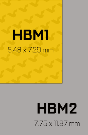
HBM2 size.
hbm2-vs-hbm1-size-comparison.png


Using 4 stacks will take up quite some space. Its for example impossible size(read interposer) wise to retrofit Fiji with HBM2, assuming its pin compatible.

I would tilt more towards a 2048bit bus now with 2 stacks.