The first Apple A10x Geekbench4 score?

Page 3 - Seeking answers? Join the AnandTech community: where nearly half-a-million members share solutions and discuss the latest tech.

Roland00Address

Platinum Member
Dec 17, 2008
2,196
260
126
Do you have any idea what 6100-U would clock in that form factor? LOL!

15w core i5s and i7s are the same silicon as the 4.5 w core m. Same die from the factory. The package is different but the package is not what makes the cpu fast.

9%20-%20Scale.jpg


Note the BGA 1515 package is using the same silicon die as the 2+2 die that BGA 1356 uses. Now this above picture is skylake but it does not change with kabylake.
 

Nothingness

Platinum Member
Jul 3, 2013
2,405
735
136
15w core i5s and i7s are the same silicon as the 4.5 w core m. Same die from the factory. The package is different but the package is not what makes the cpu fast.

Note the BGA 1515 package is using the same silicon die as the 2+2 die that BGA 1356 uses. Now this above picture is skylake but it does not change with kabylake.
FIVR was talking about the device form factor, not about the CPU/SoC packaging :)
 

Eug

Lifer
Mar 11, 2000
23,586
1,000
126
OK We finally have confirmation from Chipworks that the A10X was built on the TSMC 10nm process. The die size for the processor is 96.4 mm2.

http://techinsights.com/about-techinsights/overview/blog/10nm-rollout-marching-right-along/

"This is an impressive full node scale, when accounting for the extra CPU cores built into the A10X and extra IP blocks of the A10 vs. A9 family. We estimate a 45% die level scale (0.55x the area of running on the previous technology), based on our detailed floorplan analyses of the Apple A-series."

It would be nice if Anandtech could complete a timely analysis on the functionality of both the A10 and A10X sometime in the not too distant future. However, it seems the site is pretty resource constrained trying to keep up with everything AMD, Intel and others are doing.
So does this mean TSMC is roughly in the same ballpark as Intel as of today for process for chips of this calibre? Or are they effectively still a node shrink behind (despite the nomenclature)?
 

Roland00Address

Platinum Member
Dec 17, 2008
2,196
260
126
FIVR was talking about the device form factor, not about the CPU/SoC packaging :)

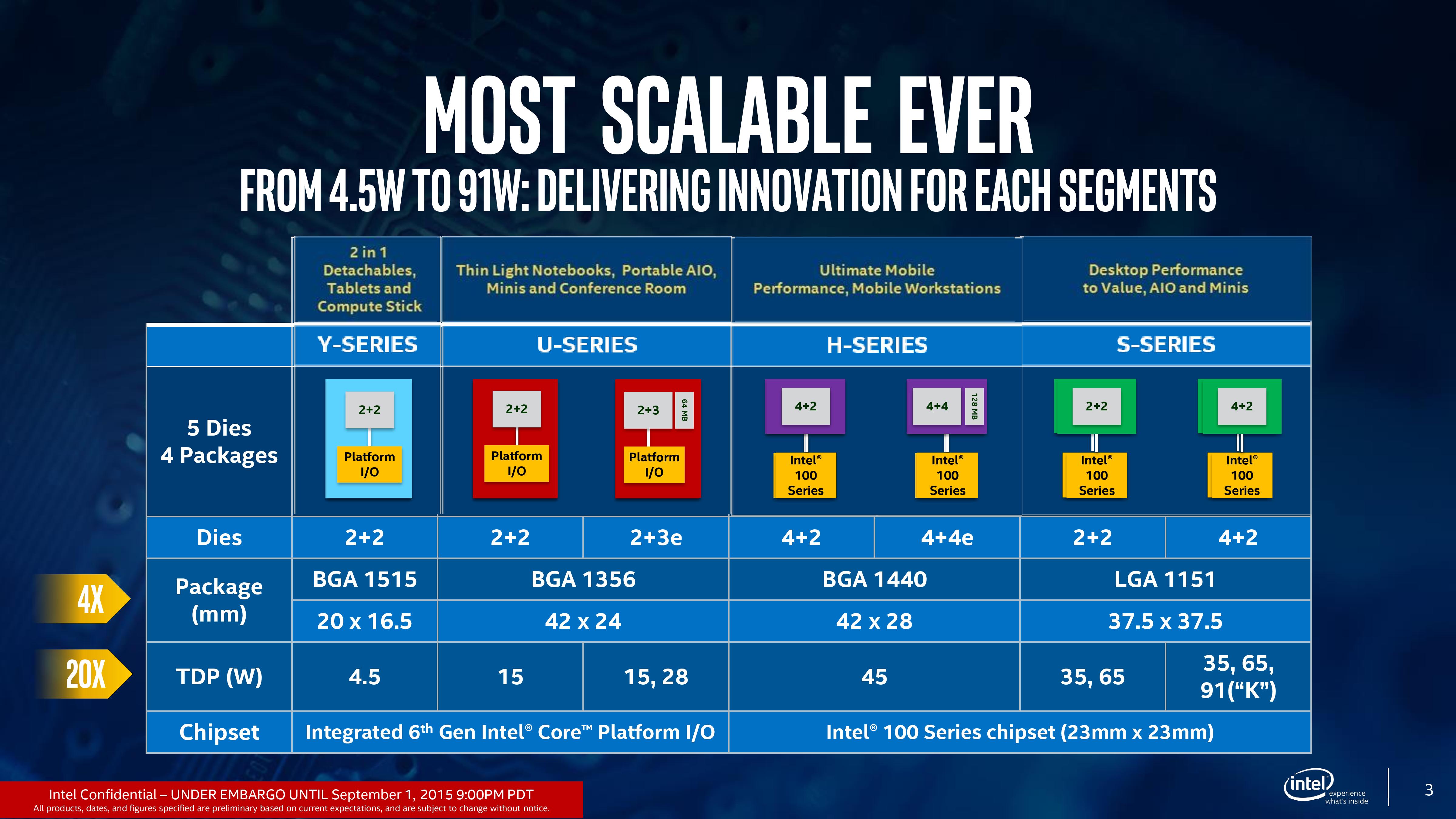
Yeah my point is the core m 4.5w processors and the core i 15w processors are really the same thing. Thus we can make those comparisons there really is very little difference with a core i3 6100u at a steady ghz vs the core m that is clocked lower but turbos to the same frequency or higher (and in some models can sustain this turbo indefinitely)

If the goal is thickness and form factor than we are getting 7 mm thickness with the core m such as the ASUS Transformer 3 T305 CA which is 6.9 mm thick. Now if the skylake / kabylake cpus have a kickstand the thickness goes up to 9 or 10 mm thick but this includes the built in kickstand and once you add the ipad's smart keyboard it is going to be just as thick.

- - - - - -

Personally I think the apple Ipad Pros and the associated apple socs are beautiful hardware. I am not dissing them in the slightest and I am simply in awe of them. That said intel also has pretty good hardware and the hardware is competitive with features, speed, etc.

Only think it is lacking is battery life and even here it is not a bad story but just as not as nice as story as the apple ipads. Then again how much of this battery life story is controlling the OS at a molecular level, in addition having far more control of what 3rd party software is allowed on it, and how many things are running in the background. An OS designed to be "open with unlimited 3rd party apps / software" and a hodgepodge of hardware and drivers is just going to find it harder to reach what you can do with a vertically integrated company with a set amount of options on the hardware, specific fine tuned drivers in regards to battery life, restricted apps and multitasking and so on. Case in point, put one of the apple ios 11 betas on the ipad and suddenly a large drop in battery life occurs. A beta is not designed for optimized battery life and you get an idea of how the difference of what you can do with the same hardware but more optimized firmware, software, etc can affect battery life.
 

Roland00Address

Platinum Member
Dec 17, 2008
2,196
260
126
So does this mean TSMC is roughly in the same ballpark as Intel as of today for process for chips of this calibre? Or are they effectively still a node shrink behind (despite the nomenclature)?

Depends on how you count. But more or less yes the 3 big foundries are in roughly comparitive feature and process sides right now. Intel may still be ahead but it is not a full node a head anymore.

Intel has been shipping 14nm and 14nm derivatives for several years now. 10 nm TSMC gets a node size with similar features on a size level as intel 14nm. That said what is die size and process node, does size matter anymore, or is the electrical properties more important? I would argue that it is more important to look at things like the power draw of the silicon, and the frequency targets you can do on a specific node is more important and that is something that is a lot more complicated with comparisons than just quoting the dimensions of a gate you can do when talking die size. But besides being harder to compare (what a process allows you to do electronically) a node may have several derivatives where on version, 2, 3, 4, and so on you get better performance than the 1st generation of what that node was shipping months or years earlier. This is the case with intel, samsung, and tsmc.

But regardless Intel has not moved onto the new 10nm node and is still stuck in its 14nm derivatives. TSMC is now shipping 10nm hardware (with features comparable and sometimes superior to intel's 14nm) and Samsung did similar 10nm hardware with its Exynos version of the Samsung Galaxy S8.

Intel is not a node ahead anymore, and that is a big deal.
 

Lodix

Senior member
Jun 24, 2016
340
116
116
Current 10nm process from Samsung and TSMC are denser than Intel's 14nm and even more compared to the recent 14nm++. By the time Intel has proper volumen for their 10nm process node competition will move to their next "7/8"nm node.
 
  • Like
Reactions: dark zero

Roland00Address

Platinum Member
Dec 17, 2008
2,196
260
126
Current 10nm process from Samsung and TSMC are denser than Intel's 14nm and even more compared to the recent 14nm++. By the time Intel has proper volume for their 10nm process node competition will move to their next "7/8"nm node.

Like I said before, depends on how you count :cool:

Remember this is not a race with a finish line, this is a marathon and just because someone is in the lead for a brief moment does not mean he will be in the lead in one time unit later (time unit being whatever, let's say a year is a time unit that is relevant)

The big deal though is not where Intel, TSMC, Samsung, etc is right this very second, but the fact that Intel is not in the lead with a complete node ahead of the competition. Right now they are neck in neck (via some counts), and some counts put Samsung and TSMC at a slight favorite but still within the margin of error... at this very moment of a temporary time.

And like I said before density is not the only thing you should judge a node by. The characteristics of the node from an electrical standpoint also matter and arguably these are things in TSMC and Samsung column as well from my understanding. Sure Intel may clock higher overall, but right now the market is not reward maximun ghz frequency with more revenue but instead other characteristics like better battery life, power efficiency in servers with clock speed vs power draw, and so on.
 

Eug

Lifer
Mar 11, 2000
23,586
1,000
126
Sure Intel may clock higher overall, but right now the market is not reward maximun ghz frequency with more revenue but instead other characteristics like better battery life, power efficiency in servers with clock speed vs power draw, and so on.
I just returned my 7700K to buy a 7600, to decrease CPU temps and fan noise. In iMacs, the fan system is apparently the same regardless of the CPU used. The 7700K isn't a great one for all-in-one systems. The cooling system cools the 7700K just fine, but isn't exactly quiet when at max.

Too bad they don't sell the 7700 in the 27" size. That's what I might have bought.
 
Mar 10, 2006
11,715
2,012
126
...And A11 is just 3 months away at the most. Even a mere 10% ST uplift from A10X is gonna smoke anything else in perf/W.

Yup. Interesting how A10X got such a nice single core perf boost mainly from going from 3MB shared L2 cache among two cores -> 8MB of L2 cache shared among three cores.

In single-threaded scenarios a single core has access to that big, fat L2 cache all to itself.
 

dark zero

Platinum Member
Jun 2, 2015
2,655
138
106
Current 10nm process from Samsung and TSMC are denser than Intel's 14nm and even more compared to the recent 14nm++. By the time Intel has proper volumen for their 10nm process node competition will move to their next "7/8"nm node.
The problem is that if someone reaches 7 nm EUV, is over for Intel since EUV is the real deal and is real 7 nm. How it performs is another story.
 

Lodix

Senior member
Jun 24, 2016
340
116
116
The problem is that if someone reaches 7 nm EUV, is over for Intel since EUV is the real deal and is real 7 nm. How it performs is another story.
SS/TSMC/GF are all targeting EUV to lower masks count and complexity of their processes at 2019. I don't think there is any "real" process since Intel will launch their 7nm process around 2020-21 and it will be denser than current "7nm".
 
Last edited:

jpiniero

Lifer
Oct 1, 2010
14,585
5,208
136
SS/TSMC/GF are all targeting EUV to lower masks count and complexity of their processes at 2018.

I am not sure about SS, but GF and TSMC are not using EUV in their first iteration of what they are calling 7 nm.