
[Techpowerup] AMD "Zen" CPU Prototypes Tested, "Meet all Expectations"
Page 20 - Seeking answers? Join the AnandTech community: where nearly half-a-million members share solutions and discuss the latest tech.
You are using an out of date browser. It may not display this or other websites correctly.
You should upgrade or use an alternative browser.
You should upgrade or use an alternative browser.
Fanatical Meat
Lifer
- Feb 4, 2009
- 35,862
- 17,407
- 136
I no longer use AMD for motherboard/cpu or graphic cards these days which is easier to keep up on the Intel and Nvidia products I use and recommend whenever I build a system.
Unfortunately I agree too many gotcha things you can get caught up in. Graphics not so much AMD doesn't work as good but its priced better.
DrMrLordX
Lifer
- Apr 27, 2000
- 23,191
- 13,275
- 136
you can pretty much consider both doubled( varies from instruction to instruction, 0% more fp div for example) but integer was significantly more bottlenecked to begin with.
Okay, I hadn't really paid good attention to the integer side of things.
Most of the time, the extra multi-threaded performance is all you need. Games and many browser benchmarks, however, do not scale well, if at all, so higher IPC is certainly more desirable.
Right . . . it's just that when you go with a CMT design ala AMD, you're sort of stuck in a situation where most of your advantage (if any) over Intel's SMT design only shows up when you load down the entire CPU with threads. Intel SMT-based designs scale up wonderfully with threads until the thread count equals the number of physical cores (scaling past that is lackluster). With SR and XV, scaling is much more even.
So when dealing with the Construction CPUs, it's kind of hard to make IPC comparisons or ever reasonably expect that their "ST" performance will every be that good, when the modules themselves are essentially designed to handle threads in pairs.
I saw a 35W Excavator to 9.85% better. I think The Stilt's numbers are TDP limited, so aren't valuable for direct comparison to higher power Steamroller parts.
No, The Stilt has a cTDP-unlocked dev platform. It's sole power limitation is the power brick. We benched head-to-head with SR (A10-7700k) vs XV (FX-8800P) @ 3.4 GHz, no turbo/no throttling. Clockspeeds remained constant. R10 saw a 5% gain, y-cruncher and AMD Linpack saw ~11%, and 3DPMRedux saw 22%.
Not gonna happen. I don't think AMD could make Zen slower than Excavator if they tried.
That was my impression, which is why I think Nosta is not accurate in his statement about 1c/2t Zen being 40% faster than an XV module limited to one thread (given the same clockspeed).
Up until examining the pipeline assignments I was certain AMD would have an inferior SMT design, but I seriously think they have the potential to match, or even exceed, Hyperthreading.
AMD has, at its option, the ability to crib from Intel's and/or IBM's SMT implementation. Or they could innovate in their own direction. It'll be interesting to see how that winds up.
I no longer use AMD for motherboard/cpu or graphic cards these days which is easier to keep up on the Intel and Nvidia products I use and recommend whenever I build a system.
That's . . . fine, though I don't see how your comment really contributes to this thread.
That's the reason why I brought this up and mentioned $/perf/W, too. As posted earlier, HSW doing heavy HPC stuff (Livermore loops) has a power consumption comprised of ~75% fixed cost / static power (burnt anyway if not power gated) and 25% caused by instruction execution itself. A large part of that fixed cost is caused by the big core: 256b wide datapaths, avx2 prfs, wide decoders, lots of heavily mixed issue ports etc.
If AMD created a small core (I'm right in the analysis phase of this hypothesis), this mix could shift to their advantage.
No, you are not right. We are not in the infancy of the power gating, it's already a very established feature and one feature that Intel processors simply excel. By going with a weaker core and having to add more to reach the same throughput doesn't remind you of something? You are basically saying that by going with a smaller core AMD will have enough advantage to offset intel power gating on the cases not optimal for Intel architectures (which will have to be optimum for Zen) and that the handicap where all units on Intel processors will be used Zen won't be at much handicap.
Tell me, do you really believe this is slightly possible? don't forget it's AMD we're talking about, not Apple, not Samsung, not Qualcomm, not IBM, not SUN. AMD.
Besides having seen ring busses mentioned somewhere in AMD patents/research publications, I think they might do an hierarchical approach + maybe rings somewhere. They might create 4C+L3 slice blocks and combine them + GPU + MCs + NB + SB via a new XBar or a ring bus.
Oh, meaning a complex cache structure in order to offset the poor interconnect. I'm feeling a dejá vu right now.
mysticjbyrd
Golden Member
- Oct 6, 2015
- 1,363
- 3
- 0
I no longer use AMD for motherboard/cpu or graphic cards these days which is easier to keep up on the Intel and Nvidia products I use and recommend whenever I build a system.
So what you are saying is that your opinion should be ignored. Gotcha.
itsmydamnation
Diamond Member
- Feb 6, 2011
- 3,123
- 3,975
- 136
how do you power gate 1/2 a dath path?No, you are not right. We are not in the infancy of the power gating, it's already a very established feature and one feature that Intel processors simply excel
No what he is saying is that for x64int, x64fp , mmx , SSE1/2/3... AVX 128 amd will have more execution units. For AVX256 and FMA they will have less throughput per core. For Server and consumer workloads this is a good trade off.. By going with a weaker core and having to add more to reach the same throughput doesn't remind you of something? You are basically saying that by going with a smaller core AMD will have enough advantage
how many server workloads use AVX256 or FMA, think mail server, web servers, DB servers, sharepoint, enterprise application servers. The answer is not very many.
again how do you power gate 1/2 a data path, 1/2 an adder, 1/2 a div or mul unit.to offset intel power gating on the cases not optimal for Intel architectures (which will have to be optimum for Zen) and that the handicap where all units on Intel processors will be used Zen won't be at much handicap.
Why not, looks at the components of bulldozer to excavator, the prefetchers/predictors, decoders, schedulers, PRF and load store system, etc are all quality. As i have said before im willing the bet a lot of these components will be evolutions of these parts or parts from jaguar.Tell me, do you really believe this is slightly possible? don't forget it's AMD we're talking about, not Apple, not Samsung, not Qualcomm, not IBM, not SUN. AMD.
We know what the execution resources look like, so that leaves the caches.
Oh, meaning a complex cache structure in order to offset the poor interconnect. I'm feeling a dejá vu right now.
Who knows the reason for the interconnect style they choose on bulldozer, jaguar shows that amd can do sain cache designs. Ring bus wont scale and a mesh wont scale so what do you propose other then some multihop design,
looncraz
Senior member
- Sep 12, 2011
- 722
- 1,651
- 136
Unfortunately I agree too many gotcha things you can get caught up in. Graphics not so much AMD doesn't work as good but its priced better.
That's actually been the opposite of my own experience. nVidia shoves in more features more often, before they are ready, which breaks builds or causes other problems. AMD hardware pulls more juice, but usually works just as well, if not better, and their drivers don't have any forced additions which cause headaches (at least thus far
 ).
).Once upon I time, of course, this was not the case, but it very much has been since the 5000 series and the catalyst rewrite.
Then again, I have a strict policy regarding updates: security updates only, unless something is broken, then wait until the one fix that helps you. Otherwise, I only update with major versions.
Of course, I ran BeOS as my main operating system until 2009 or so :thumbsup:
how do you power gate 1/2 a dath path?
again how do you power gate 1/2 a data path, 1/2 an adder, 1/2 a div or mul unit.
For AVX, pretty trivially. The 128-bit halves of the AVX instruction are physically separate. This is the reason why real world SIMD instruction sets are allergic to cross-lane operations, even though any good programmer can tell you that cross-lane operations are very useful.
AMD already had a similar design in BD -- each SSE pipe had two floating point units, one 80 bits (for x87) and one a little over 64. Combined, they worked on 128-bit quantities.
Intel design hasn't been published afaik, but Agner Fog's work has shown that full sustained 256-bit throughput is only available thousands of cycles of ramp-up. This is consistent with a design where half of the SIMD unit is powered off until the CPU is working on a workload where it's worth it to power it up.
Just to extend: Part of the foundational idea of SIMD, that makes it worth it to actually implement in silicon instead of more scalar units despite it's inflexibility, is that while each lane of a SIMD array receives identical instructions, there doesn't need to be any cross-lane communication which means that the individual lanes can be physically very far from each other, allowing more efficient data routing and easier layout. This also allows efficient partial use of SIMD arrays.
Dresdenboy
Golden Member
Hehe, did I say, that I'm right about something? I just brought some points up. Power gating comes with a cost in cycles (as mentioned by Tuna-Fish). Clock gating is the method, which can be done on a per cycle basis.No, you are not right. We are not in the infancy of the power gating, it's already a very established feature and one feature that Intel processors simply excel. By going with a weaker core and having to add more to reach the same throughput doesn't remind you of something? You are basically saying that by going with a smaller core AMD will have enough advantage to offset intel power gating on the cases not optimal for Intel architectures (which will have to be optimum for Zen) and that the handicap where all units on Intel processors will be used Zen won't be at much handicap.
Tell me, do you really believe this is slightly possible? don't forget it's AMD we're talking about, not Apple, not Samsung, not Qualcomm, not IBM, not SUN. AMD.
My point is not about power gating (did I mention this? sorry then). It's about scaling (128b -> 256b SIMD vs. 1 core -> 2 cores).
Here's the Intel paper:
http://kentcz.com/downloads/P149-ISCA14-Preprint.pdf
and the slides:
http://kentcz.com/downloads/ISCA149_slides_final.pdf
The way the AVX units were used here didn't give power gating a chance.
Interesting are mentions like energy efficiency of HSW over Penryn improved 20% (everything else normalized).
Last edited:
Dresdenboy
Golden Member
Isn't using SIMD also a way to reduce the instruction management overhead/execution ratio?Just to extend: Part of the foundational idea of SIMD, that makes it worth it to actually implement in silicon instead of more scalar units despite it's inflexibility, is that while each lane of a SIMD array receives identical instructions, there doesn't need to be any cross-lane communication which means that the individual lanes can be physically very far from each other, allowing more efficient data routing and easier layout. This also allows efficient partial use of SIMD arrays.
looncraz
Senior member
- Sep 12, 2011
- 722
- 1,651
- 136
AMD already had a similar design in BD -- each SSE pipe had two floating point units, one 80 bits (for x87) and one a little over 64. Combined, they worked on 128-bit quantities.
I thought it was 64+64, with both ganging for anything larger (incl 80-bit), which was why code with x87 instructions performed so relatively poorly. I seem to remember something AMD no longer making special hardware just for x87.
Dresdenboy
Golden Member
There are 80 bit wide paths (+margin).I thought it was 64+64, with both ganging for anything larger (incl 80-bit), which was why code with x87 instructions performed so relatively poorly. I seem to remember something AMD no longer making special hardware just for x87.
Hiroshige Goto published the detailed FPU description from an AMD ISSCC paper back then.
looncraz
Senior member
- Sep 12, 2011
- 722
- 1,651
- 136
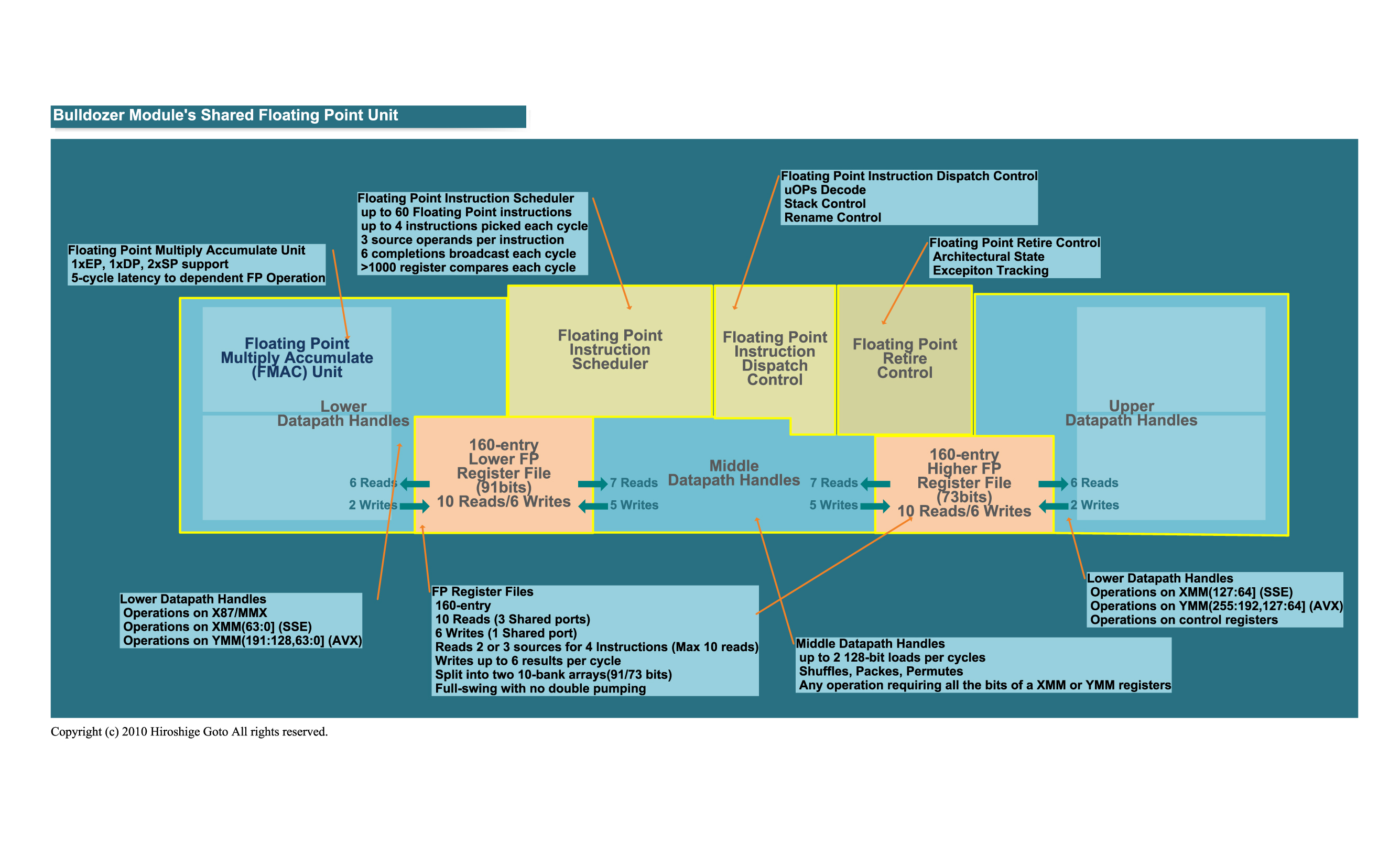
There are 80 bit wide paths (+margin).
Hiroshige Goto published the detailed FPU description from an AMD ISSCC paper back then.
I see, 91+73. Surprised I never noticed that
I guess this is it?
Dresdenboy
Golden Member
Yep. There is another one, more like an overview:I see, 91+73. Surprised I never noticed that
http://pc.watch.impress.co.jp/img/pcw/docs/430/341/11.jpg
Isn't using SIMD also a way to reduce the instruction management overhead/execution ratio?
Yes.
I thought it was 64+64, with both ganging for anything larger (incl 80-bit), which was why code with x87 instructions performed so relatively poorly.
The point in having the two pipes is that they are far apart from each other in silicon. (And in fact, even their register files are far apart in silicon.) This means they can't be ganged together to work on things where results require information from both halves. Horizontal ops in BD all have latency of at least 10 cycles, while x87 ops add/mul are 6. They have extra bits over the 64/80 so that they can do full-precision division using the FMA pipes in less cycles, and so that they don't have to deal with denormals except during load/store. (I actually thought they only had 80 bits on the fat side and handled x87 denormals in microcode like a lot of older CPUs, but apparently they wanted them to be faster than that.)
BD is comparatively worse in x87 (and even in a lot of old SSE code) because they did away with separate add/mul units and just have FMA pipes. This is good for throughput, but terrible for latency-sensitive code that has a lot of fadds as the latency of fadd is now the latency of FMA.
Dresdenboy
Golden Member
This was a reminder, because this ratio could also be changed by reducing the overhead.Yes.
Small core hypothesis. I'm now at ~5mm² incl. L2 and somewhat over 3mm² w/o L2. This might change a little bit with ongoing research and more information becoming available.
Last edited:
Matthias
Be sure to post here when you have an update !
http://dresdenboy.blogspot.dk/2015/10/amds-zen-core-family-17h-to-have-ten.html?m=1
Keep up the good work
Be sure to post here when you have an update !
http://dresdenboy.blogspot.dk/2015/10/amds-zen-core-family-17h-to-have-ten.html?m=1
Keep up the good work
Cloudfire777
Golden Member
- Mar 24, 2013
- 1,787
- 95
- 91
Notice that the work on 16nm Zen ended before the summer of 2015. We know it taped out shortly after. The 14nm SOCs are currently under development (began May this year)

14nm SOC design/Cheetah is this one
14nm SOC design/Cheetah is this one
Wait, 14/16nm Cat cores are still happening? Whaaat
It's probably for the consoles.
Consoles, embebbed and AM1+! If that is true AM1+ is still alive, but maybe targeted only to low cost machines until their successor appears.Wait, 14/16nm Cat cores are still happening? Whaaat
Also Cat cores aren't based on BD cores, but maybe a revamp is comming up.
Finally, since Zen is only CPU is logic that movement (and Raven Ridge will come 2017+ and Stoney Ridge only goes up to 2016, there is no successor). So maybe Cheetah is targeting notebooks and AM1+ (since they didn't confirmed their death) and Tiger are going after consoles.... Hexa Core time maybe? R5 time?
So.... Zen is based somehow in Cat Cores.....
I don't think Zen is based on Cat cores. I also think that the future cat cores aren't targeting anything but the consoles that already exist.
Both the current-gen consoles have relatively large and power-hungry chips. As soon as the new processes are mature enough, the vendors definitely want to switch over. I expect that the next-gen cat cores are just straight up shrinks that actually try very hard not to have *any* performance change upon the past gen, other than lower power at same performance.
There being two projects means that they want to be able to manufacture Jaguar derivates both on TSMC and on Samsung/GloFo. I wonder if the console vendors went with different foundries, or if either of them wanted to have ability to dual-source.
monstercameron
Diamond Member
- Feb 12, 2013
- 3,818
- 1
- 0
Notice that the work on 16nm Zen ended before the summer of 2015. We know it taped out shortly after. The 14nm SOCs are currently under development (began May this year)
14nm SOC design/Cheetah is this one
Nosta, why you hack his account XD.
cbn
Lifer
- Mar 27, 2009
- 12,968
- 221
- 106
Notice that the work on 16nm Zen ended before the summer of 2015. We know it taped out shortly after. The 14nm SOCs are currently under development (began May this year)
14nm SOC design/Cheetah is this one
Wait, 14/16nm Cat cores are still happening? Whaaat
Here is what I found when I searched the term AMD cheetah:
http://wccftech.com/amd-developing-...-arm-cores-features-gcn-20-cores-hsa-support/
Cheetah With GCN 2.0, HSA+ and Massive Compute Capabilities
Regardless of the process design, AMD’s x86 Cheetah architecture would introduce new technologies geared towards compute. It is clearly mentioned that AMD’s x86 Cheetah cores won’t be enough to power compute needs which the APU is geared towards, hence for each CPU core there would be one dedicated 64-bit ARM core that analyses the incoming tasks & offloads them to the GPU. This is obviously not as efficient as running tasks that are using OpenCL (or any GPU acceleration), but it works with every application so even older programs like an old video editor or a pure CPU benchmark will use the GPU to do most of the work.
The x86 Cheetah core architecture would also be highly scalable with different products in 2, 4, 6, 8 x86 core variants. Since each CPU core has one dedicated ARM core, we are also looking at 2,4,6,8 ARM cores on the x86 Cheetah based APUs. The single-threaded performance of these next-generation APUs would be better then past generation cores since the ARM cores would be able to offload tasks to the GCN cores while the other cores stay in idle state to conserve power.
The Cheetah based APUs would be geared towards consumers first and hence it will feature GCN 2.0 graphics core architecture. The amount of GCN 2.0 cores is the multiple of the amount of x86 cores which essentially means that an 8 Core model will have 8 x86 Cheetah cores, 8 ARM cores and several GCN compute units which will span the low-end mobility to the most high-end desktop SKUs. The Athlon equivalent of the core would adopt around 128-384 GCN processors while the high-end variants can include upto 1024 stream processors and clock speeds of around 900-1000 MHz. The specifications for SKUs aren’t finalized yet but we are looking at a top-to-bottom SKU lineup featuring the Cheetah and GCN 2.0 core design.
The APU will give the ability to set the maximum amount of GPU cores being used for GPGPU computing through AMD drivers because the more GPU cores assigned to help the CPU, the less cores will be available for the “real” GPUtasks, although a “dynamic” scaling system is in planning as well. AMD has also developed a bypass for GCN cores which can now be used coherently with a discrete graphics card. Previous generation APUs disable the iGPU when the system is running on dedicated graphics except for a few Dual Graphics solution options available on the Radeon R7 lineup. With Cheetah APUs, this limitation will be bypassed an all integrated GCN 2.0 cores would be scheduled to handle GPGPU computing while the dedicated GPU will work along side to handle GPU tasks.

AMD is also allegedly planning to introduce HSA+ solution or Advanced HSA on their next generation x86 and ARM based APUs. The new HSA set will enable that all x86 cores, ARM cores and GPU cores would be able to share the main memory in a coherent manner rather than just the main x86 cores and GPU.
The x86 Cheetah cores and APU are currently under research and development phase and it would be some time before they see the light of day and most probably under a different name. But the recent ambidextrous project roadmap highlights that AMD is giving a strong emphasis to APU and SOC featuring both ARM and x86 cores on the same die and that is where their future lies.
The source was also keen to share details that AMD is very well planning a new x86 high-performance core which will mark the return of FX series in 2015-2016 with much better performance obtained through an architecture built from the ground up and that GCN 2.0 architecture is coming this year. We have an article on that coming up soon but the details mention that GCN 2.0 is not much powerful in terms of GPGPU computation but provides a huge jump in power efficiency. So the next two- three years for AMD really sound great and stay tuned for more information.
TRENDING THREADS
-
 Discussion Zen 5 Speculation (EPYC Turin and Strix Point/Granite Ridge - Ryzen 9000)
- Started by DisEnchantment
- Replies: 25K
-
Discussion Intel Meteor, Arrow, Lunar & Panther Lakes + WCL Discussion Threads
- Started by Tigerick
- Replies: 24K
-
 Discussion Intel current and future Lakes & Rapids thread
- Started by TheF34RChannel
- Replies: 23K
-

-

AnandTech is part of Future plc, an international media group and leading digital publisher. Visit our corporate site.
© Future Publishing Limited Quay House, The Ambury, Bath BA1 1UA. All rights reserved. England and Wales company registration number 2008885.