[Sweclockers] SK Hynix is showcasing next-gen HBM memory for Nvidia's Pascal

Page 3 - Seeking answers? Join the AnandTech community: where nearly half-a-million members share solutions and discuss the latest tech.

DiogoDX

Senior member
Oct 11, 2012
757
336
136
OK, well I guess you could in theory call 2.5D interpose "3D memory" since the memory itself is stacked vertically. However, a logical definition of "real" 3D memory is 3D Vertical Stack directly on top/underneath the GPU; and this is the definition AMD agrees with too. That's coming with Volta in 2018, not Pascal, and yet NV wants to market Pascal with "3D memory" which sounds misleading indeed.

For me 3d memory is a "cube" (3d plain) made by stacking dram chips. HMC and HBM are types of 3d memory. Each stack (4hi, 8hi) is a 3d memory by definition.

3d stacking is simply placing the stack on top of the gpu/soc.
 

RussianSensation

Elite Member
Sep 5, 2003
19,458
765
126
For me 3d memory is a "cube" (3d plain) made by stacking dram chips. HMC and HBM are types of 3d memory. Each stack (4hi, 8hi) is a 3d memory by definition.

3d stacking is simply placing the stack on top of the gpu/soc.

Ok fair enough. So then Pascal will have 3D memory, configured as a 2.5D stacked configuration. :p
 

HurleyBird

Platinum Member
Apr 22, 2003
2,800
1,528
136
Evergreen's memory controller was flat out superior to Fermi's, but I think it's too close to call a winner in terms of GCN vs. Kepler. If history repeats itself, AMD will have a far superior HBM2 controller vs. Pascal and Nvidia will catch up with Volta.
 

cmdrdredd

Lifer
Dec 12, 2001
27,052
357
126
HBM has higher bandwidth, lower latency, uses half the power of GDDR5 and reduces the space taken up by the die, will make for smaller, simpler PCBs, will run cooler.

Please tell me it was smart for Nvidia to stick with GDDR5 for 2015 instead of HBM. We have no idea what other changes AMD have done to the architecture now that they have 50% more bandwidth to take advantage of it.

Maybe cost savings for them to use proven tech now and wait for the next iteration? Dunno.
 

Cookie Monster

Diamond Member
May 7, 2005
5,161
32
86
You confused me. You said the exact same thing as me, but in different words. I just said that the complexity of the memory controller determines how well it can hit higher clocks because you can easily source 5-8Gbps GDDR5 chips. The more complex the memory controller, the harder it is to achieve higher clocks speeds. That's been the general rule for AMD/NV for several generations, but it's not always 100% true as I've shown with 384-bit 7970 hitting 365GB/sec!

You forgot that having a 512bit bus doesnt necessarily mean a more complex memory controller. You've shown an example that some cards are able to hit high clocks. But just how many can run stable at those clocks? That is the impressive part because all nVIDIA parts run at ~7GHz reference speeds another ~1GHz headroom.

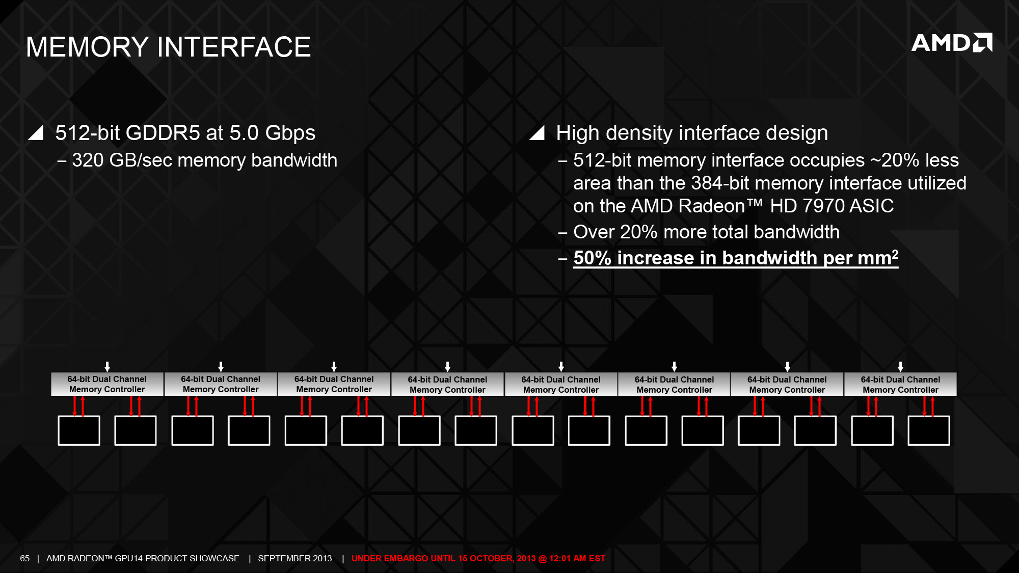
No, they would not. That's the #1 misconception for Hawaii. AMD reduced the memory controller's die size area by 20% from Tahiti's 384-bit bus and because the controller is 512-bit, they used less power hungry / slower GDDR5 chips. The end result is 50% increase in memory bandwidth/mm2. That's engineering winning 101. Your suggestion that AMD would have been better off with a 256-bit or a 384-bit memory controller on 290X doesn't fly. 290X keeps up with 780Ti despite VASTLY superior DP performance, similar perf/watt, and a 438mm2 die size vs. 561mm2 die size for Kepler GK210!

A 256bit memory bus will always mean less memory controllers (smaller die size and complexity), less PCB complexity and i.e. potentially less layers, less power required for the memory bus/ic because you only need 8 of them compared to 10, 12 and so forth.

Why doesnt it fly? As long as it has enough bandwidth, the GPU would definitely be smaller, less transistors and cheaper. Every cent counts. The PCB itself too would be cheaper. If theres no performance benefit in going with a 512bit bus over a 256bit where bandwidth is assumed same why would anyone go with the former? because it sounds nice on paper?

And by power hungry, just how much is that difference?

So it's clear that when comparing efficiency per mm2 of 2 head-to-head competing architectures (290X vs. 780Ti), Hawaii completely smashed its direct competition!! AMD engineers designed a crazy efficient 512-bit memory controller which allowed for 290X to be just 438mm2, or just 24% larger in die size than a 7970, but pack 50% more memory bandwidth and 37.5% more functional units (SPs and TMUs), with 100% the ROPs! That's incredible in hindsight.

This sounds like some sort of AMD PR. Comparing die sizes is also futile mainly because AMD may have gone with a more dense/compact layout plus the architecture is completely different. The more meaningful comparison should be, "..they've added 50% more memory with 37.5% more functional units by adding approx. 44% additional transistors..". ~44% increase in transistors for ~50% across the board which sounds about right. Die size won't be increased by 50% either because the amount of space taken up by each block is different.

It is impressive in terms of how well its faring still to this day (games that favor this arch also helps) but it is not impressive when you start playing with its headroom and the kind of power consumption figures it has. Why do you think it has a bad rep even to this day?

From an engineering point of view (SP/DP/compute/& perf/mm2), 290X is by far superior to a 780Ti. Just think about it, a 550mm2 is what 390X is rumoured to be which is another way of saying if you scale Hawaii 290X to 550mm2, how would the 561mm2 780Ti compare? It wouldn't stand a chance! All this time NV has been 'lucky' that AMD wouldn't have the b**lls to make a 500mm2+ GPU. Once that happens, NV's 15-20% historical advantage is going to disappear.

Memory.jpg

The only reason they haven't done that is a) yields, b) too power hungry c) cost. Theres greater risk involved when it could perform less than its competition and AMD cant afford those ever (hence why they took the small die strategy). Same thing can happen with nVIDIA but they can take one or two missteps thanks to their superior financial position.

Its interesting how you compare Kepler with Fiji and call that impressive.. Its like saying "look how great maxwell is vs tahiti!". Its also uncharacteristic of you to start using terms like luck(?)..

NV might hold an advantage in more efficient colour compression, but not the design of the memory controller. As I already said, 290X matches or beats 780Ti in performance despite a 438mm2 die size, but still packs a ton of DP performance, and a 512-bit memory controller. Despite a 561mm2 die, 780Ti could only manage a 384-bit memory controller, far inferior SP and DP performance and can't even outperform the 290X!

Maybe because bandwidth is not the primary contributor for overall performance? I have no idea what DP performance and die size has anything to do with memory controller performance. One good metric is how high they can be clocked and we all know nVIDIA parts are clocked at high stock memory clocks (and have plenty of headroom). AMD's memory controller may well be smaller and use less transistors is also their advantage.

About the only thing 780Ti can rightfully claim over 290X from an engineering point of view is about an 11% advantage in perf/watt at 1440/4K. That's nothing, considering AMD's engineers designed a way better all-around gaming+compute chip at only $550, gave it 4GB of VRAM and packed it in a die size just 78% the size of 780Ti's. That's why members on our forum who are so quick to write off AMD by comparing Maxwell against the outdated R9 200 series and not understanding just what AMD engineers were able to achieve with a 290X are going to be for a major surprise when 390X drops.

Last time I checked, nVIDIA holds a dominant position over the discrete GPU market share along with the workstation/GPGPU market..? Designing a better all around product is good on paper, but for the application is it really required? Does Hawaii need DP capabilities that it has now? What if having a 1/32 rate on Hawaii resulted in the card being ~200W only? What then? I feel really bad for them because they must be selling most of their R290 at cost price!

Plus you cannot stop the comparisons to maxwell either because it is here now with many different types of SKU and AMD has yet to release anything.

Just wait until 390X - it should level the Titan X in perf/mm2, SP and DP compute performance, and provide > 50% the memory bandwidth and you'll see just how good AMD can design the memory controller. :p

That's why this idea that Pascal will use HBM2 but AMD won't is some fluffy BS alright.

Im not sure about the last statement but the FP64 capability in Fiji might hurt in terms of power consumption if the same ratio is kept as Hawaii. I can't think of many games that even require DP. It'd actually be more beneficial for them to just limit them like maxwell to save power for their gaming line.

And Id have no idea if their memory controller is better or not. Why? Its HBM vs GDDR5. Not even comparable. Once we get Pascal based cards, maybe then there could be some meaningful comparisons between the two.
 

0verl0rd

Junior Member
May 1, 2015
1
0
0
Nvidia makes the smarter and better choice of waiting for HBM2.

32GB of HBM2 memory in 4 stacks(8GB stack x 4) for Pascal Quadro & Tesla cards since those customers keep on needing more memory to handle their complex workloads.

16GB of HBM2 memory in 4 stacks(4GB stack x 4) for Pascal TITAN class card as halo flagship design.

8GB of HBM2 memory in 4 stacks(2GB stack x 4) for Pascal GeForce gaming cards.

lol, like how some people try to spin failure to deliver a product as smart! Nvidia bet on now delayed Volta & HMC memory. They didn't wait for HBM2, they're waiting now because they have to, as AMD have a clause with Hynix deal.

Here's Nvidia's scrapped 2013 roadmap http://icpp2013.ens-lyon.fr/GPUs-ICPP.pdf
 
Last edited:

Azix

Golden Member
Apr 18, 2014
1,438
67
91
Nothing there indicates Gen2 is NVidia exclusive.

In fact, common sense would indicate it isn't.

yeah but now less common sense persons will see nvidia in even better light. Its all a conspiracy.

On some forum somewhere someone is telling others that nvidia is so uber cool with HBM2 1TB/s bandwidth....

Nvidia makes the smarter and better choice of waiting for HBM2.

32GB of HBM2 memory in 4 stacks(8GB stack x 4) for Pascal Quadro & Tesla cards since those customers keep on needing more memory to handle their complex workloads.

16GB of HBM2 memory in 4 stacks(4GB stack x 4) for Pascal TITAN class card as halo flagship design.

8GB of HBM2 memory in 4 stacks(2GB stack x 4) for Pascal GeForce gaming cards.


Nvidia didn't make a choice, they had none. Their cards are coming out before the tech was ready. AMD is right at the start for GPUs using it. Naturally nvidias next gpus will likely come before AMDs so they will use hbm2 first if its ready.

HBM2 fits Nvidia's needs better than HBM and I never stated anything about AMD, seriously everyone here in this forum seems to have a beef to pick with anything.

Why? because they don't have hbm1? There are a few people going about saying everything nvidia is doing or has to do due to lack of choice is just better and due to their overwhelming godlike GPU prowess. Sometimes, they just have no choice. If they could have they would have jumped on it obviously
 
Last edited:

Azix

Golden Member
Apr 18, 2014
1,438
67
91
Use HBM now and be limited to 4GB on Quadro, Tesla & GeForce cards? Thats a good laugh.

AMD may be first to GDDR5 but their GDDR5 controllers sucks and is power inefficient and can't support higher speeds compared to Nvidia's GDDR5 controller that can run at 7GHZ & even supports 8GHz memory speeds.

http://www.anandtech.com/show/5699/nvidia-geforce-gtx-680-review/2


Nvidia will have the better memory controller again for HBM era.

I'm not getting why it sucks. AMD generally has better bandwidth than nvidia. They just approach it differently. Does the memory really consume more from 384bits + 7GHz to 512bits + 5GHz? lower clocking VRAM chips are probably an advantage in costs too.
 
Last edited:

Erenhardt

Diamond Member
Dec 1, 2012
3,251
105
101
Use HBM now and be limited to 4GB on Quadro, Tesla & GeForce cards? Thats a good laugh.

AMD may be first to GDDR5 but their GDDR5 controllers sucks and is power inefficient and can't support higher speeds compared to Nvidia's GDDR5 controller that can run at 7GHZ & even supports 8GHz memory speeds.

http://www.anandtech.com/show/5699/nvidia-geforce-gtx-680-review/2


Nvidia will have the better memory controller again for HBM era.

You are reaching new heights of ridiculousness.


AMD memory controllers reach speeds as high as nvidias.
7GHz and more

gpuz_oc.gif
 
Last edited:

RussianSensation

Elite Member
Sep 5, 2003
19,458
765
126
You are reaching new heights of ridiculousness.

AMD memory controllers reach speeds as high as nvidias.
7GHz and more

3 years ago HD7970's 384-bit memory controller could go > 7Ghz.

54_sap797oc1_gpu-z_big.png

Source

Of course this amount of memory bandwidth is overkill for a card as slow as a 7970 and it wasn't commercially viable to sell all 7970s with such high GDDR5 speeds due to yields and increased power usage.

As far as that poster goes, he constantly hyped up everything NV and downplays all AMD's new tech. This reminds me of certain users on our forum talking smack about R9 390X "requiring" AIO CLC while ignoring the huge benefits it offers, while quietly buying the AIO CLC for their 980/Titan X cards. :D
 

cmdrdredd

Lifer
Dec 12, 2001
27,052
357
126
I guess it depends on the gpu in use. If you cannot make usage of the extra bandwidth then it serves no purpose. So a 7970 like you said at 7ghz memory wouldn't make use of the bandwidth at all would it?
 

RussianSensation

Elite Member
Sep 5, 2003
19,458
765
126
I guess it depends on the gpu in use. If you cannot make usage of the extra bandwidth then it serves no purpose. So a 7970 like you said at 7ghz memory wouldn't make use of the bandwidth at all would it?

That's true but HBM brings many other advantages. Ask yourself this, does a GP200 Pascal need nearly 2.25-3X the memory bandwidth of Titan X? Chances are NV can easily provide it with 750GB/sec-1TB/sec courtesy of HBM2. Will GP200 need that much bandwidth? Probably not because it's likely it will use a 4th generation memory bandwidth compression technology on top of Maxwell's 3rd gen.

One of the major advantages of HBM is reduction in PCB size to just 1/3 of the current size! How is this possible? Because you are moving the GDDR5 spread out all over the PCB onto the interposer/much closer to the GPU itself. Think about how large of a PCB you'd need to have a GPU with 32GB of VRAM? This also poses a dilemma because if GDDR5 density is not there yet, you physically can't even make a card with 32-64GB of VRAM. HBM also reduces latency.

Nvidia-Pascal.png


hbm12.jpg


It's going to allow for GP200 with 250W TDP to be a miniITX card assuming you strap an AIO CLC to cool it.

Lets be honest here. Many (most?) 7970s did not get over 7 ghz on the vram.

That's not the point. A certain poster alluded that AMD cards can't operate at high GDDR5 speeds because their memory controllers are inferior. He was proven wrong. There is obviously a great engineering reason for NV and AMD to not pursue 512-bit memory controllers paired with 8Ghz GDDR5 and power usage is one of the main factors. Since NV's Maxwell architecture with its large L2 cache was extremely power efficient, they didn't have an urgent task to squeeze every ounce of perf/watt. AMD didn't spend 3-4 years designing a brand new architecture for R9 300 series which means they had to find other ways to improve perf/watt --> that's where HBM1 comes in. Since NV knows that making a 512-bit memory controller with 8Ghz GDDR5 is highly inefficient, they will also adopt HBM but by late 2016, we'll have HBM 2.0 which is why NV will skip HBM 1. Both strategy makes sense for their respective designs. Hypothetically speaking, had NV used HBM 1 for Titan X, the card would have been even more power efficient.
 
Last edited:

3DVagabond

Lifer
Aug 10, 2009
11,951
204
106
Lets be honest here. Many (most?) 7970s did not get over 7 ghz on the vram.

Maybe that has more to do with the spec of the RAM not the limit of the memory controller? Besides, it has nothing to do with nVidia. nVidia obviously isn't using HBM either because it wasn't ready in time, or they aren't ready to use it yet. It doesn't really matter though. Either way, they aren't using it.
 

Enigmoid

Platinum Member
Sep 27, 2012
2,907
31
91
Maybe that has more to do with the spec of the RAM not the limit of the memory controller? Besides, it has nothing to do with nVidia. nVidia obviously isn't using HBM either because it wasn't ready in time, or they aren't ready to use it yet. It doesn't really matter though. Either way, they aren't using it.

My point is (and its a minor rather subtle one) that you cannot take a specific example and apply in in the general case. Most haswell chips don't overclock well (compared to sandy); the fact that someone has a golden 5.0 ghz 4770k does not invalidate this point. The fact that a few 7970s overclock high on the RAM does not mean the the memory controller of all chips can take those high frequencies. (Looking on HW bot - I have no clue how accurate this is - the Vram overclock for the 680 is significantly faster than the 7970). This might be vram chips and NOT the memory controller.

This is not really important and I don't want to argue. My point was just the properties of a picked specific golden example does not apply to every other dull penny.
 

Techhog

Platinum Member
Sep 11, 2013
2,834
2
26
The first generation HBM will allow much greater speeds compared to GDDR5. The four layer stack, also known as 4-Hi, will pack either 1GB or 2GB capacity. The eight layer stacks (8 Hi) are also planned.

So, I guess this confirms that HBM1 (and thus Fiji) is limited to 4GB...
 

RussianSensation

Elite Member
Sep 5, 2003
19,458
765
126
So, I guess this confirms that HBM1 (and thus Fiji) is limited to 4GB...

AMD is rumoured to be employing a technology by SK Hynic called a “Dual Link Interposer” which will allow memory capacities upwards of 8GB without the use of 2nd Generation HBM. 2x 4-HI HBM1 (which should technically be called 8-Hi-Hi according to nomenclature rules) features a 1024-bit interface, two prefetch operations per IO (dual command) and can push 128GB per second per pin. The tRC is 48nm, tCCD is 2ns (1tCK), and VDD is 1.2V. The 4-Hi HBM2 (generation 2) features a 1024 bit interface, two prefetch operations per IO (dual command), 64 Byte access granularity (=I/O x prefetch) and can push 256 GB per second per pin. The tRC is 48nm, tCCD is 2ns (1tCK), and VDD is 1.2V.
 
Last edited:

wilds

Platinum Member
Oct 26, 2012
2,059
674
136
I'm interested to see how much power these HBM modules save in real-world scenarios. 4 GB of high-speed HBM could be fantastic in a thin gaming notebook.
 
Last edited:

5150Joker

Diamond Member
Feb 6, 2002
5,549
0
71
www.techinferno.com
Really AMD has no choice but to release an 8 gb top model so if the technology to do it is available, they can license it. The question remains how large of an impact this will be overall in terms of performance. Top GPUs don't gain much from faster memory, even at high resolution. If they're doing it to improve perf/watt then it makes more sense. Maybe even long term cost reduction would be a factor to use it.
 

stahlhart

Super Moderator Graphics Cards
Dec 21, 2010
4,273
77
91
Thread cleaned. All of you get a second chance to discuss "dual-link interposer", this time without violating posting rules.
-- stahlhart