I wouldn't be so sure about that. I think its almost entirely related to the memory controller and the bus design/layout not the actual VRAM IC itself. Your also forgetting that its not just 1x512bit memory controller but made up of say 8x64bit memory controllers. Id think its more to do with how well an individual memory controller can handle the higher clocks because the rest are just duplicates of itself.
You confused me. You said the exact same thing as me, but in different words. I just said that the complexity of the memory controller determines how well it can hit higher clocks because you can easily source 5-8Gbps GDDR5 chips. The more complex the memory controller, the harder it is to achieve higher clocks speeds. That's been the general rule for AMD/NV for several generations, but it's not always 100% true as I've shown with 384-bit 7970 hitting 365GB/sec!
If AMD had the chance of going 256bit and a higher clocked part, they would most definitely taken that route because complexity as a whole goes down i.e. cost.
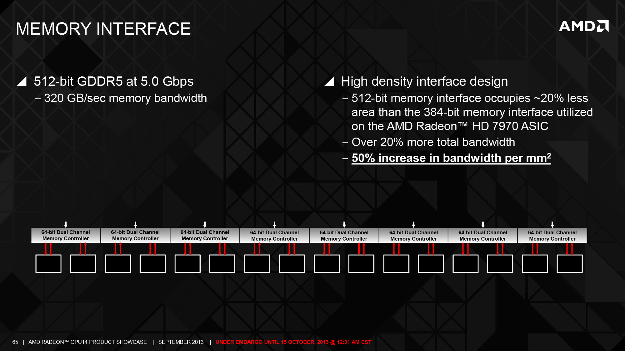
No, they would not. That's the #1 misconception for Hawaii. AMD reduced the memory controller's die size area by 20% from Tahiti's 384-bit bus and because the controller is 512-bit, they used less power hungry / slower GDDR5 chips. The end result is 50% increase in memory bandwidth/mm2. That's engineering winning 101. Your suggestion that AMD would have been better off with a 256-bit or a 384-bit memory controller on 290X doesn't fly. 290X keeps up with 780Ti despite VASTLY superior DP performance, similar perf/watt, and a 438mm2 die size vs. 561mm2 die size for Kepler GK210!
So it's clear that when comparing efficiency per mm2 of 2 head-to-head competing architectures (290X vs. 780Ti), Hawaii completely smashed its direct competition!! AMD engineers designed a crazy efficient 512-bit memory controller which allowed for 290X to be just 438mm2, or just 24% larger in die size than a 7970, but pack 50% more memory bandwidth and 37.5% more functional units (SPs and TMUs), with 100% the ROPs! That's incredible in hindsight.
From an
engineering point of view (SP/DP/compute/& perf/mm2), 290X is by far superior to a 780Ti. Just think about it, a 550mm2 is what 390X is rumoured to be which is another way of saying if you scale Hawaii 290X to 550mm2, how would the 561mm2 780Ti compare? It wouldn't stand a chance! All this time NV has been 'lucky' that AMD wouldn't have the b**lls to make a 500mm2+ GPU. Once that happens, NV's 15-20% historical advantage is going to disappear.
I think nVIDIA do hold an advantage here hence why they are constantly getting away with lower memory bus width than the competition.
NV might hold an advantage in more efficient colour compression, but not the design of the memory controller. As I already said, 290X matches or beats 780Ti in performance despite a 438mm2 die size, but still packs a ton of DP performance, and a 512-bit memory controller. Despite a 561mm2 die, 780Ti could only manage a 384-bit memory controller, far inferior SP and DP performance and can't even outperform the 290X!
About the only thing 780Ti can rightfully claim over 290X from an engineering point of view is about an
11% advantage in perf/watt at 1440/4K. That's nothing, considering AMD's engineers designed a way better all-around gaming+compute chip at only $550, gave it 4GB of VRAM and packed it in a die size just 78% the size of 780Ti's. That's why members on our forum who are so quick to write off AMD by comparing Maxwell against the outdated R9 200 series and not understanding just what AMD engineers were able to achieve with a 290X are going to be for a major surprise when 390X drops.
Just wait until 390X - it should level the Titan X in perf/mm2, SP and DP compute performance, and provide > 50% the memory bandwidth and you'll see just how good AMD can design the memory controller.

That's why this idea that Pascal will use HBM2 but AMD won't is some fluffy BS alright.