Why the assumption on fixed SMT values? I thought that IBM has long used a 'scaling on the fly' SMT variation, so we know it works. An up to SMT4 core 'as needed' might be the better solution.
Its a half node but I think there's a significant gain in density compared to 7nm that Zen 2 is using. Its not double but there seems to be room for AMD to increase the size of the chiplets (especially on EPYC and Threadripper). Plus, AMD will likely be changing packaging (i.e. socket) somwhere in there as well as shrinking the size of the I/O die, so they could increase the chiplet sizes themselves. And there's other aspects they can likely play with (shape of the chiplets as well for instance).
Something I've been curious about (since I've been pushing for it a lot), due to the recent GF announcement about their new version of 12, including a new interposer for HBM (which I think HBM3 is supposed to be made on 12nm, so I'm still left wondering, what if they integrated the HBM into/on say the I/O die itself, skipping the interposer entirely), would slapping some of that with the I/O die let them reduce cache sizes? That'd let them increase core counts and/or size of the cores. Which, yes it'd be higher latency than L1, L2, and maybe L3 cache (although I think it'd be not that far off from the latter), but that could possibly be mitigated via the throughput (bandwidth), and pooling the cache (so perhaps there could be some smart sharing of resources that would mitigate latency issues). But maybe they could keep L1 and L2 cache low, replace L3 with a larger pool of HBM, which could double as buffer to system RAM and maybe even NAND, so that you're increasing the throughput significantly (more than making up with the slightly reduced latency).
Slightly off topic, but I'm actually wondering if ARM's Cortex A78/Hercules might be SMT2, with a 6 wide core it would certainly be interesting to see how much they can get out of it considering what they already managed on a 3 wide core (A65/E1/Helios).I'm more interested in if they can squeeze more performance out of SMT2. Currently, AMD's implementation of SMT2 is good for maybe a 25-30% increase in throughput. In theory they should be able to get more out of it on a wider core.
Eh? All GPGPU code is software, technically all graphics GPU code is software too - the driver shader compiler just obfuscates that from the user.No SW GPGPU needed
Slower than L3 for sure, but a damn sight lower latency than DDR mounted on the motherboard, not to mention lower power draw too as the distance is so much less to travel - if they ever mount HBM on the CCX chiplets it would make a killer L4.HBM is way to slow compared to L3 cache, for example. The latency difference is huge (don't have the numbers on me, but HBM is at least an order of magnitude slower and would have to route through the IO chip to service all CCXs).
Arm pretty much stated that they have absolutely no plans to ever adopt SMT in any IP going into battery powered devices.Slightly off topic, but I'm actually wondering if ARM's Cortex A78/Hercules might be SMT2, with a 6 wide core it would certainly be interesting to see how much they can get out of it considering what they already managed on a 3 wide core (A65/E1/Helios).
I found it odd that they announced their first SMT design on a Little core (even if it is 3 wide OoO), and then announced no follow up big core this year.
Shame if so, seems like a waste with that 6 wide core.Arm pretty much stated that they have absolutely no plans to ever adopt SMT in any IP going into battery powered devices.
And AMD can implement HW bypass for calculation on GPU.
I ment to bypass compilers and go directly into HW. Something like GPU front-end will able to decode AVX512 a calculate it. There would be some latency penalties however for large vectors it can be much faster.Eh? All GPGPU code is software, technically all graphics GPU code is software too - the driver shader compiler just obfuscates that from the user.
Unless you mean for the shader compiler to be entirely hosted by the hardware, like the change to hardware scheduling?
It might be sort of like GPU microcode.
I'm probably talking completely out of my ass here of course, feel free to say as much!
The purpose of mobile Big cores is to deliver peak IPC. If you would adopt SMT2 you can gain 30% more throughput (130% total) however your performance per thread will fall down to 65% (130% divided by 2 threads). This doesn't make sense when for efficiency you have LITTLE cores. It's very interesting that mobile ARMs never implemented SMT - It looks like SMT has more disadvantages than benefits for mobile market.Shame if so, seems like a waste with that 6 wide core.
To be fair, A65/E1/Helios with SMT only got announced last year - I wouldn't take ARM's word as gospel that we will get no SMT mobile core ever.It's very interesting that mobile ARMs never implemented SMT - It looks like SMT has more disadvantages than benefits for mobile market
I'm pretty sure he meant an APU, so basically infinity fabric - it will be no worse than going from chiplet to chiplet, perhaps better if they implement it directly on the CCX chiplet itself, though I admit to a healthy skepticism about this ever happening however tempting it sounds to indulge in the speculation.There are many reasons why they haven't done that already. Latency is an issue when dealing with a PCIe-connected GPU.
This was a whole era at AMD's. It started with the merge of ATi in 2006. We almost immediately got the mighty Fusion branding (The Future is Fusion!), followed with M-SPACE in 2007.Though before Bulldozer came out, there was a PR image released about future APU design, in 3 parts.
Part 1 showed entirely separate CPU and GPU, the pre Llano days.
Part 2 showed 2 big chunks of CPU and GPU next to each other in a way that basically echoes all APU's today.
Part 3 showed a distributed mix of GPU bits in amongst the CPU bits, in what I would assume to be a far off future design.
Now obviously the utter failure of Bulldozer will have derailed any far off designs based on it in favor of fixing bugs and clawing back perf/watt, but that doesn't necessarily mean that the meat of that mixed design may not still materialise in the future (assuming it wasn't merely a graphics wingding by an unusually hopeful soul in the PR department).
Today it's basically a non existent terminology, the Boltzmann Initiative provided the HIP compiler, and the genesis of ROCM and at that point it basically became a runtime/SDK for that - and it's still not even available on Windows to my astonishment.just to rebrand it to today's HSA year later
That can be attributed to AMD having to near completely abandon it due to Bulldozer's repeated problems and the consequential Zen fast track soaking up R&D budget - almost certainly the reason also that there was no post Piledriver server chip before Epyc landed.13 years after the Fusion announcement, an average enduser is lucky if he/she uses a single OpenCL-backed app which doesn't treat the integrated GPU in any special way. Don't trust the marketing hype. Such is life.
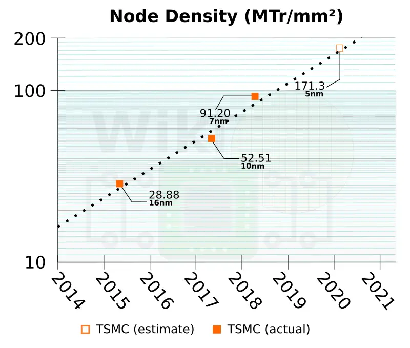
Well, I checked an article on Wikichip and was shocked to see that, according to TSMC's estimate, density will increase by approximately 85%!
This is probably for SRAM, so logic may not scale quite as well.
This give AMD allot of xtors to play with for Zen4. A 20% bump in chiplet size would double the number of CCXs per CCD, if AMD wants to go that way.
AMD may want to go for a wider core and increase cache instead. Lots of decisions to be made (well, AMD has already made them!).
HBM is way to slow compared to L3 cache, for example. The latency difference is huge (don't have the numbers on me, but HBM is at least an order of magnitude slower and would have to route through the IO chip to service all CCXs).
Similarly GCN is a truly sorry mess of lost opportunities, because AMD lacked the budget freedom to pursue a more aggressive software development initiative to make it as attractive as CUDA solutions for professionals.
That's not how that works, not at all.From what I can gather GCN was at least as competitive as Fermi derivatives in sheer compute power per watt for it's reign of Southern Islands to Vega
They now have the HIP API as a real alternative to the CUDA API. Modern C++ features, single-source programming model (OpenCL and all PC gfx APIs are separate-source models), and it's a true low level API since HIP kernels are directly compiled into native GCN hardware bytecode and no intermediate representations/languages are used like as seen with examples such as HLSL shaders -> DXBC/DXIL, Metal shaders -> Apple IR (intermediate representation), OpenCL Kernels -> SPIR/SPIR-V kernels, Vulkan shaders -> SPIR-V shader or even CUDA kernels -> PTX ...
That's because density is the primary quality of any node. Density and performance are two sides of the same coin. Starting with a high density, improving the performance by reducing the density again in specific areas is how it's usually achieved. Intel's different 14nm(++) optimizations are just that.They seemed to have focused a lot on density as power and performance don't go up nearly as much. I'm assuming there's a reason for that.
Yes, and?That's not how that works, not at all.
Peak FP != compute.
In WASM's case I think it also gives smaller code, though I could be wrong there.Compiling to a bytecode is a feature, not a bug. It gives you portability and forwards compatibility.
Compiling to a bytecode is a feature, not a bug. It gives you portability and forwards compatibility.
Peak FP != compute.a superior compute power which was largely a missed opportunity
You keep making an obvious point about something I was not arguing against in the first place.Peak FP != compute.
Hammer that into your brain already.