Speculation: Ryzen 4000 series/Zen 3

Page 21 - Seeking answers? Join the AnandTech community: where nearly half-a-million members share solutions and discuss the latest tech.

Ajay

Lifer
Jan 8, 2001
15,332
7,792
136
If we're lucky, AMD will double the number of FMACs and support AVX512 through op fusion ala Zen/Zen+.
How about not double the FMACs an just use op fusion for one AVX512 stream (just for compatibility).
AVX512 is such a power sink :screamcat:
 

DrMrLordX

Lifer
Apr 27, 2000
21,570
10,763
136
How about not double the FMACs an just use op fusion for one AVX512 stream (just for compatibility).
AVX512 is such a power sink :screamcat:

Doubling the # of FMACs would improve AVX2 performance. Yes, it's a power sink, but the extra performance would be worth it for people that need it. I don't think AMD is going to just stop at allowing one AVX512 stream; why switch to 512-bit FMACs when they can go for groupings of 2x256-bit instead? Yes, AMD would be slower in AVX512 thanks to op fusion overhead, but they'd wind up faster in AVX2.
 

itsmydamnation

Platinum Member
Feb 6, 2011
2,731
3,063
136
You still need to load and store all this data, a simple doubling of fmac's without significantly larger data paths/PRF/retire isn't going to be worth it and increasing all of those is going to make a very big core ( lets not forget how big sunny cove is).
 
  • Like
Reactions: NTMBK

DrMrLordX

Lifer
Apr 27, 2000
21,570
10,763
136
You still need to load and store all this data, a simple doubling of fmac's without significantly larger data paths/PRF/retire isn't going to be worth it and increasing all of those is going to make a very big core ( lets not forget how big sunny cove is).

That's correct. AVX512 is coming though, like it or not.

I guess they could just use op fusion to support AVX512 and call it a day, which would be fine from my point-of-view. I just don't think they'll go that route. They're getting a small density increase with 7nm+.
 

itsmydamnation

Platinum Member
Feb 6, 2011
2,731
3,063
136
That's correct. AVX512 is coming though, like it or not.
I don't really think it is, if your code can scale to 512bit vectors linearly it most likely can scale more cores as well. Having more high clocking high IPC lower width cores, then less lower clocking lower IPC 512bit wide cores will work better for far more workloads/environments.
 

DrMrLordX

Lifer
Apr 27, 2000
21,570
10,763
136
I don't really think it is, if your code can scale to 512bit vectors linearly it most likely can scale more cores as well.

Sometimes yes, sometimes no. It didn't stop Intel from pushing it though. That is the #1 reason why AMD will adopt it, at least for a time. Hopefully AVX512 can be unseated by something like SVE2 in the future.
 

soresu

Platinum Member
Dec 19, 2014
2,582
1,778
136
All of that is possible, and someone academic at this point unless some version of XOP emerges in the future. Personally I'd like to see AMD throw out AVX altogether in favor of SVE2 but . . . that's unlikely to happen. Instead we're probably going to see AVX512 support in Zen3 which is not thrilling. But Intel has moved the market in that direction, so I guess AMD needs to follow.
It's not impossible, and certainly preferable to have SVE2 style variable vectors, unless there are specific restrictions in the x64 ISA preventing it.

RISC-V also has a length agnostic vector instruction set in development, it seems the natural evolution for vector computing, if perhaps not so easy to implement.

Though I might add that I believe SVE was based on a research paper detailing an instruction set called ARGON - this paper implied diminishing returns past a point, so unless they addressed that problem in subsequent research, there won't be a great amount of mileage beyond 512 bit length vectors.
 

soresu

Platinum Member
Dec 19, 2014
2,582
1,778
136
Instead we're probably going to see AVX512 support in Zen3 which is not thrilling
Unlikely after a mere 20% area reduction unless their SIMD unit design is incredibly area efficient - they just doubled FP with Zen2 as it is, adding AVX-512 without that increase would be similar to having AVX2 before Zen2.

Perhaps we may see it with Zen3 if a significant core redesign opens up some space, but more likely with Zen 4 at 5nm I think.

Not to mention their current core per socket advantage does offset AVX 512 some, as shown by their stellar SVT-AV1 encoding results with EPYC 7742.

512 bit code isn't nearly as prevalent yet too - even Intel had to add 256 bit code to SVT-VP9, which had the side effect of boosting EPYC too.
 
Last edited:
  • Like
Reactions: amd6502

moinmoin

Diamond Member
Jun 1, 2017
4,926
7,608
136
What about if AMD will create shared front-end for whole CCX? This would bring some advantages out of CMT while still using SMT for back-end.
1) This could save some transistors and increase throughput.
2) It allows HW control over threads within CCX. It can eliminate crazy windows scheduler shuffle.
I myself was previously toying with the thought of moving some of the front end's functionality onto the IOD even. Problem is always data locality, you don't want to move critical data too far away from where it's actually needed to keep latency down.

Maybe the decoder could be situated before the core specific front end, so that all instructions hitting L2/3$ are already in the optimized internal uop format. Branch prediction, specifically TAGE that relies on long histories to work ideally, could also profit from being handled centrally. But aside latency to make efficient use of such a topology the task scheduler would need to be moved from OS into hardware, and that's something which for AMD's RTG repeatedly turned out to be a hindrance instead an advantage compared to Nvidia's driver controlled scheduling. On the other hand centralized hardware scheduling would allow for clean separation of INT and FP units as well as making HSA more feasible again. But as of now all of that is not feasible and won't happen.

Unlikely after a mere 20% area reduction unless their SIMD unit design is incredibly area efficient - they just doubled FP with Zen2 as it is, adding AVX-512 without that increase would be similar to having AVX2 before Zen2.
512bit FP can still happen by the way of combining the two 256bit FMACs already there. The issue with AVX-512 are all the additional instructions that are then also usable with 128bit and 256bit FP and likely need quite some area as well.

Zen 4 on 5nm with up to 50% higher density (compared to 7nm+, up to 80% compared to 7nm) could allow a bigger increase in transistors again, allowing another doubling of the FP unit with accordingly widened data paths/loads/stores etc.

It was mentioned before that many changes to the Zen 2 core were initially planned for Zen 3, so I'm expecting the Zen 3 core to be a much more polished coherent implementation of many parts that were premiered in Zen 2 (aside FP the newly introduced TAGE branch predictor is a primary candidate for such).
 
  • Like
Reactions: amd6502

moinmoin

Diamond Member
Jun 1, 2017
4,926
7,608
136
She was definitely an important part (team leader), however chief architect was Mike Clark.
It looks like different people are leading the different Zen gen efforts as chief architect. Zen 1 was Mike Clark. Zen 2 was David Suggs. And according to his LinkedIn profile (via wccftech, sorry) Suggs apparently also handles Zen 5.
 
  • Like
Reactions: amd6502

NTMBK

Lifer
Nov 14, 2011
10,208
4,939
136
Sometimes yes, sometimes no. It didn't stop Intel from pushing it though. That is the #1 reason why AMD will adopt it, at least for a time. Hopefully AVX512 can be unseated by something like SVE2 in the future.

Intel pushed it as a way to boost their Larrabee derivatives. The theory was that if mainstream CPUs shared an ISA with the Phi, they could get a critical mass of compatible software.

Of course it never really panned out, and now Phi is dead. I don't really see the benefit to huge vectors which are so power hungry that they tank the performance of the rest of your CPU. I mean great, you boosted peak FLOPs, but now all the logic you need to get data to feed those vector units is running at a crippled clock speed.

AVX-512 as an ISA has some really nice features like mask registers and full masking of pretty much every instruction, and scatter to match the gather instructions from AVX2. It makes it a much better ISA to vectorize for. But I'd be happy with it on half width vector units.
 

amd6502

Senior member
Apr 21, 2017
971
360
136
You are right, Nehalem had 3xALU.
I agree that 6xALU or 8xALU design are the next step as the lowest hanging fruit.


I think 5 or 6 ALU is likelier in Zen3. I think we could see 6 ALU in Zen4, and not ruling out we might see 8 ALU.

And again I'm pushing my hope that SMT will make symmetry optional (with an aSMT mode). Linux is already ready for asymmetric cores, although it seems application for it so far is for mosly for telephones.


utilization clamping support as an extension of their work on the Energy Aware Scheduling framework in order to boost some workloads while capping background workloads.
(from https://www.phoronix.com/scan.php?page=news_item&px=Linux-5.3-Scheduler-Clamping ).

Low ipc non-speculative logical cores would be the most low energy and secure way to process threads.
 
Last edited:

Richie Rich

Senior member
Jul 28, 2019
470
229
76
I think 5 or 6 ALU is likelier in Zen3. I think we could see 6 ALU in Zen4, and not ruling out we might see 8 ALU.

And again I'm pushing my hope that SMT will make symmetry optional (with an aSMT mode). Linux is already ready for asymmetric cores, although it seems application for it so far is for mosly for telephones.


(from https://www.phoronix.com/scan.php?page=news_item&px=Linux-5.3-Scheduler-Clamping ).

Low ipc non-speculative logical cores would be the most low energy and secure way to process threads.
IMHO AMD will keep ALU core fixed for whole family. Same as 17h Family Zen1+2 was 4xALU core design fixed. They also kept 4 pipes for FPU, just doubling width of FPUs. On the other hand they added one store unit, but I consider this as minor back-end change - probably eliminating bottleneck of AGUs with no impact to front-end.

IMHO 19H Family will keep 6xALU number fixed too. At least for Zen3, Zen4 and Zen5.

There is rumour about 15 chiplets for server Zen3 Epyc Milan. I think it isn't possible put there 14 CPU chiplets with 8 cores. I think this is another indirect evidence that Zen3 core will be big beast core. If Zen3 core will be estimated 6xALU core with 8 FPU pipes and 4xAGU + SMT4, this means this core will consists of approximately +50% more transistors, so quad-core CCX will be much larger than Zen2 (chiplet die area 80 -> 120mm2).


AMD can create 1xCCX chiplet which can cut the die area down to 60mm2 and receive better yields and binning.
  • - Zen2 ROME: 8 chiplets x 8 core CCD x 2 SMT => 64c/128t (perf 100% ST, 100% MT)
  • - Zen3 MILAN: 14 chiplets x 4 core CCX x 4 SMT => 56c/224t (perf 150% ST, 175% MT)

Die areas also looks good:
  • - Zen2 Rome 8x80mm2 = 640mm2,
  • - Zen3 Milan 14x60mm2 = 840mm2 (x0.9 EUV factor= 756mm2).Pretty similar.

This allows to use big 14nm IO die as interposer for HBM on it. Oh god, if this will be true then this is game over for Intel.

Do you remember Lisa Su's words? "Just for the record, zero truth to this rumor (leaving AMD). I love AMD and the best is yet to come!" She was IMHO talking about new uarch 19h Family Zen3.
 

Richie Rich

Senior member
Jul 28, 2019
470
229
76
I myself was previously toying with the thought of moving some of the front end's functionality onto the IOD even. Problem is always data locality, you don't want to move critical data too far away from where it's actually needed to keep latency down.

Maybe the decoder could be situated before the core specific front end, so that all instructions hitting L2/3$ are already in the optimized internal uop format. Branch prediction, specifically TAGE that relies on long histories to work ideally, could also profit from being handled centrally. But aside latency to make efficient use of such a topology the task scheduler would need to be moved from OS into hardware, and that's something which for AMD's RTG repeatedly turned out to be a hindrance instead an advantage compared to Nvidia's driver controlled scheduling. On the other hand centralized hardware scheduling would allow for clean separation of INT and FP units as well as making HSA more feasible again. But as of now all of that is not feasible and won't happen.
Your ideas are briliant however too much futuristic. I'm talking about just share front-end in Bulldozer style. Zen4 could have CCX front-end capable to handle 16 threads, internally 4 cores 6xALU each, and shared 4x 8 = 32 pipes of 256 bit FPU. Bulldozer had very weak back-end, especially FPU was very weak. However it was not so bad thanks to sharing. If they would share strong back-end it will become even stronger.


512bit FP can still happen by the way of combining the two 256bit FMACs already there. The issue with AVX-512 are all the additional instructions that are then also usable with 128bit and 256bit FP and likely need quite some area as well.

Zen 4 on 5nm with up to 50% higher density (compared to 7nm+, up to 80% compared to 7nm) could allow a bigger increase in transistors again, allowing another doubling of the FP unit with accordingly widened data paths/loads/stores etc.

It was mentioned before that many changes to the Zen 2 core were initially planned for Zen 3, so I'm expecting the Zen 3 core to be a much more polished coherent implementation of many parts that were premiered in Zen 2 (aside FP the newly introduced TAGE branch predictor is a primary candidate for such).
Could I ask where did you get Zen4 will be 5nm? Because I assume Zen4 being equivalent for Zen1+ (plus shared front-end :D), so probably shrink to 6nm EUV. New process (5nm) I would estimate for Zen5 (Zen2 like).
 

moinmoin

Diamond Member
Jun 1, 2017
4,926
7,608
136
Your ideas are briliant however too much futuristic. I'm talking about just share front-end in Bulldozer style. Zen4 could have CCX front-end capable to handle 16 threads, internally 4 cores 6xALU each, and shared 4x 8 = 32 pipes of 256 bit FPU. Bulldozer had very weak back-end, especially FPU was very weak. However it was not so bad thanks to sharing. If they would share strong back-end it will become even stronger.
The problem I see with a combined front end for every CCX is that that approach may make disabling cores awkward. So far AMD is pretty adamant at keeping behavior and latency the same regardless of the internal topology even when a CCX contains less than 4 cores due to disabled cores. But it's certainly a more feasible approach than what I had in mind. Let's see if they do anything in that direction of combining resources across cores, the TAGE branch predictor would profit a lot from such.

Could I ask where did you get Zen4 will be 5nm? Because I assume Zen4 being equivalent for Zen1+ (plus shared front-end :D), so probably shrink to 6nm EUV. New process (5nm) I would estimate for Zen5 (Zen2 like).
TSMC offers different upgrade paths for its customers where much of the design rules are kept to keep the cost down. 6nm is the direct upgrade from 7nm (which Zen 2 uses). 5nm is the direct upgrade from 7nm+ (which Zen 3 is announced to use). A switch back to the 7nm -> 6nm upgrade path makes no sense when the most recent design (then Zen 3) already uses 7nm+ which prepares for the vastly superior 5nm node (which will be the next real deal, like the jump from GloFo's 12nm to TSMC's 7nm).

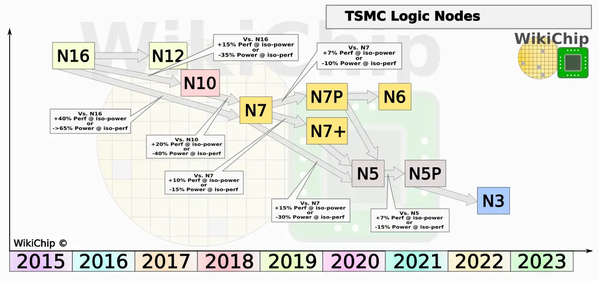
wikichip_tsmc_logic_node_q2_2019.png
 

DrMrLordX

Lifer
Apr 27, 2000
21,570
10,763
136
Wouldn't 6nm be inferior to 7nm+ for high-performance parts? I see no reason why Zen4 would move backwards to a less-performant node.
 

soresu

Platinum Member
Dec 19, 2014
2,582
1,778
136
which will be the next real deal, like the jump from GloFo's 12nm to TSMC's 7nm
Unless my math is way off, the 7nm+ to 5nm move is only a 11-11.2% power reduction, and about a 33.5-34% area reduction.
1568690825073.png
So fairly good for area, but closer to 7nm to 7nm+ for power.
 

soresu

Platinum Member
Dec 19, 2014
2,582
1,778
136
Let's see if they do anything in that direction of combining resources across cores
I haven't heard anything substantial about speculative multi-threading (SpecMT) for some time, it's a shame no-one ever managed it in practice.

Though transactional memory is supposed to be a significant part of that problem - maybe ARM's TME might be laying the groundwork for SpecMT in the future.
 

moinmoin

Diamond Member
Jun 1, 2017
4,926
7,608
136
Unless my math is way off, the 7nm+ to 5nm move is only a 11-11.2% power reduction, and about a 33.5-34% area reduction.
View attachment 10869
So fairly good for area, but closer to 7nm to 7nm+ for power.
Where is that table from? I based my math (50% higher density 7nm+ -> 5nm) on WikiChip's reporting from end of July:
"Compared to their N7 process, N7+ is said to deliver around 1.2x density improvement."
"Compared to N7, N5 is said to deliver 1.8x routed logic density."

Power and performance is then dependent on how that density is used, usually high performance areas use significantly lower density.
 
Mar 11, 2004
23,020
5,485
146
Where is that table from? I based my math (50% higher density 7nm+ -> 5nm) on WikiChip's reporting from end of July:
"Compared to their N7 process, N7+ is said to deliver around 1.2x density improvement."
"Compared to N7, N5 is said to deliver 1.8x routed logic density."

Power and performance is then dependent on how that density is used, usually high performance areas use significantly lower density.

Its from one of the Anandtech articles (I think on the one where TSMC announced the 6nm process). I think those numbers were supposedly from TSMC itself too.

I think they've since had other articles with different figures too though. Frankly, I'm not sure if they even know yet.

Its possible there was a typo or something too and the 5FF was supposed to be against 7FF+ not 7FF.

Wouldn't 6nm be inferior to 7nm+ for high-performance parts? I see no reason why Zen4 would move backwards to a less-performant node.

I'm not sure about that, but I believe 6nm is mostly about providing an easy and less expensive node for customers that care more about price than max performance related metrics. It provides some minor benefit over 7, and I think its supposed to possibly be easier to transition to (compared to 7) since it uses EUV, so if you were a company that hangs behind a node (and you're still at 16/14nm, or maybe 12 or 10nm), you might would skip 7 and go right to 6.
 
  • Like
Reactions: spursindonesia

NostaSeronx

Diamond Member
Sep 18, 2011
3,683
1,218
136
6nm is for those who want to port from 7nm DUV, but don't want to completely redesign.

RTO => Retapeout re-uses GDS, but now has EUV. Same die, no changes other than EUV adopted. <== Extra yields
NTO => Completely new tapeout, but re-uses 7nm AMS/SRAM cells, but has its own 6nm Logic cells. <== Extra logic density and yields

Only people going to 6nm are those on 7nm DUV. As 7nm+ in general for 2020+ is better in every case. There is always room for a N6+ for N7+ compatibility as well.
 

soresu

Platinum Member
Dec 19, 2014
2,582
1,778
136
Where is that table from? I based my math (50% higher density 7nm+ -> 5nm) on WikiChip's reporting from end of July:
"Compared to their N7 process, N7+ is said to deliver around 1.2x density improvement."
"Compared to N7, N5 is said to deliver 1.8x routed logic density."

Power and performance is then dependent on how that density is used, usually high performance areas use significantly lower density.

From an Anandtech article back in April (link), as darkswordsman17 says the figures were supposed to be directly from TSMC - there is also a second 5nm process called N5P with higher performance announced in late July (link), "The latter will also be offered in a performance-enhanced version called N5P. This technology will also feature FEOL and MOL optimizations in order to make the chips run 7% faster at the same power, or reduce consumption by 15% at the same clocks. "

Just scanned the WC article, not sure how Anand's and WikiChip's figures differ so much.
 

tomatosummit

Member
Mar 21, 2019
184
177
116
6nm is for those who want to port from 7nm DUV, but don't want to completely redesign.

RTO => Retapeout re-uses GDS, but now has EUV. Same die, no changes other than EUV adopted. <== Extra yields
NTO => Completely new tapeout, but re-uses 7nm AMS/SRAM cells, but has its own 6nm Logic cells. <== Extra logic density and yields

Only people going to 6nm are those on 7nm DUV. As 7nm+ in general for 2020+ is better in every case. There is always room for a N6+ for N7+ compatibility as well.
I see n6 as analogous to 12ff was to 14ff. A node refresh for customer to reuse masks, AMD could use it for a low end navi refresh in a year or so and any upcoming IO dies.
Zen3 designs will probably go ahead with n7+ as they'll be substantially new designs wanting cutting edge performance.

Isn't a lot of this all conjecture though. AMD is reported to be using "7nmHP" that isn't on tsmc's public slides so we don't know how it ports to n6 and if n7+ is or isn't a high performance node. or if there's a variant.
 

moinmoin

Diamond Member
Jun 1, 2017
4,926
7,608
136
Isn't a lot of this all conjecture though. AMD is reported to be using "7nmHP" that isn't on tsmc's public slides so we don't know how it ports to n6 and if n7+ is or isn't a high performance node. or if there's a variant.
In slides AMD has been using "7nm+" for Zen 3 for ages now. N6 was only unveiled in April. And N7 used for Zen 2 technically wasn't a "HP" node either.
 

Saylick

Diamond Member
Sep 10, 2012
3,082
6,171
136
Unless my math is way off, the 7nm+ to 5nm move is only a 11-11.2% power reduction, and about a 33.5-34% area reduction.
View attachment 10869
So fairly good for area, but closer to 7nm to 7nm+ for power.

According to Wikichip's slide of TSMC's nodes, I came to a similar conclusion as well. Note the performance gains at iso-power between N to N7+, and N7 to N5 as shown below:
wikichip_tsmc_logic_node_q2_2019.png


N7 ---> N7+ (+10% perf @ iso-power)
N7 ---> N5 (+15% perf @ iso-power)

Doesn't that imply only a 4.5% perf gain @ iso-power when we move from 7nm+ to 5nm? That's not a big jump at all, and considering that most of the time, the perf @ iso-power gains are given at the perf/W sweet-spot (i.e. not at Fmax), this really highlights Forrest Norrod's point that future node shrinks will not push the max clocks any higher with the more likely outcome being a clock regression.

For this reason, I reckon any meaningful performance gains moving forward in the next 5 years, assuming we don't switch to graphene or another semiconductor material with drastically better properties, will largely be the result of architectural improvements, likely a combination of larger cores and/or fixed function hardware.