Some Bulldozer and Bobcat articles have sprung up

Page 12 - Seeking answers? Join the AnandTech community: where nearly half-a-million members share solutions and discuss the latest tech.

Soleron

Senior member
May 10, 2009
337
0
71
AMD said two things:
- Their sheets say "Throughput advantages for multi-threaded workloads without significant loss on serial workload components".
- JFAMD says IPC will be higher.

I'm saying they're contradicting eachother. If there is a loss of throughput on serial workload components, no matter how insignificant, the IPC can not be higher.

Loss of throughput compared to two fully seperate integer cores. Not compared to Phenom II.

Imagine:

2 Phenom cores = 100% IPC

2 BD modules, 1 core per module = 130% IPC

1 BD module, 2 cores per module = 120% IPC

JF has also made two other claims with regards to performance:

1. Interlagos will perform 50% better than MC in the same thermals
2. IPC increase for single-threaded workloads will be "a lot" more than 17%
 
Last edited:

Scali

Banned
Dec 3, 2004
2,495
0
0
Loss of throughput compared to two fully seperate integer cores. Not compared to Phenom II.

As I already said:
1) There *is* no non-shared BD architecture. That means they have never made this actual comparison. It also means that any such speculation would be completely meaningless.
2) It's virtually impossible for AMD to get more IPC out of the BD architecture, since it has less execution units per thread. Worst case, BD's pipelines will have to do 50% more work than Phenom II to reach the same throughput (two units doing the work of three). They're not going to make THAT big a jump in efficiency, that's not even remotely realistic.
 

bryanW1995

Lifer
May 22, 2007
11,144
32
91
AMD said two things:
- Their sheets say "Throughput advantages for multi-threaded workloads without significant loss on serial workload components".
- JFAMD says IPC will be higher.

I'm saying they're contradicting eachother. If there is a loss of throughput on serial workload components, no matter how insignificant, the IPC can not be higher.


I think a single HT core would be smaller than a BD module. Intel also has the upper hand in single-threaded IPC, which probably will not chance. So although HT may not run two threads as effectively as BD does, the smaller size and the higher single-threaded performance may cancel out BD's 'advantages'.
Namely, HT will generally give us ~30% extra performance out of the second core...
So the total performance of a HT core would be A = 1.3*X
Now if we assume that a BD module performs like B = 1.8*Y, then A > B as long as X is big enough. Which would be ~38% bigger than Y.

Another thing is that HT is easy to scale up. Intel just has to drop in extra execution units. It's the same idea as BD, only the sharing of execution resources is 100%, and more flexible.

30 percent improvement for ht? really? I don't see anything close to that on my i7. maybe for specific usage patterns you can get "up to" 30 percent, but real world 10-15% is more like it.

scali said:
As I already said:
1) There *is* no non-shared BD architecture. That means they have never made this actual comparison. It also means that any such speculation would be completely meaningless.
2) It's virtually impossible for AMD to get more IPC out of the BD architecture, since it has less execution units per thread. Worst case, BD's pipelines will have to do 50% more work than Phenom II to reach the same throughput (two units doing the work of three). They're not going to make THAT big a jump in efficiency, that's not even remotely realistic.

so now jfamd is not just a liar but a BIG liar since he's gone on record as saying that ipc will jump more than 17%. don't you think that it's at least possible that all the engineers at amd know a bit more about cpu design than you do?
 
Last edited:

JFAMD

Senior member
May 16, 2009
565
0
0
Loss of throughput compared to two fully seperate integer cores. Not compared to Phenom II.

Imagine:

2 Phenom cores = 100% IPC

2 BD modules, 1 core per module = 130% IPC

1 BD module, 2 cores per module = 120% IPC

JF has also made two other claims with regards to performance:

1. Interlagos will perform 50% better than MC in the same thermals
2. IPC increase for single-threaded workloads will be "a lot" more than 17%

Actually I said 3 things:
1. Interlagos will perform 50% better than MC in the same thermals
2. IPC would be higher
3. Increase for single-threaded workloads will be "a lot" more than 17%

I have made no statements that I am aware of about IPC with a percentage implied because I don't know what the IPC is, all I was told is that it would be higher. If I did say IPC would be higher by a percentage, it was a mistake; ocasionally those things happen to us humans.

The ~17% number (or the 12.5% or 12.8% numbers) are all tied to people trying to reverse engineer the 50% number (performance of 16-core vs. 12-core) for a single thread. I have said repeatedly that trying to pull single thread performance from a statement about a fully loaded and fully utilized processor is not going to be accurate. It is like trying to figure out travel times at 3AM based on rush hour traffic.

Based on Scali's treatment recently I just don't feel like I need to respond to him at all. Let him think whatever he wants, it is more convenient for him that way.
 

Kuzi

Senior member
Sep 16, 2007
572
0
0
Hey Kuzi, feels like we've been talking about Bulldozer for a while now, huh ;)

Yeah IDC, and after all this time, the damn thing is still not released yet :p


So the answer - 1.8x scaling for two thread executing within the same BD module - could be the answer to any number of questions, we don't really know the precise details behind the motivating question itself.

I just took the 1.8x number as meaning this is the "Max" gain we can expect with 2 threads running per BD Module. As opposed to having a "Full" dual-core executing 2 threads which can improve performance by up to 2x.

Of course as you mentioned, it all depends on the software at hand, so the gain can be anywhere from nothing to 2x. Your graph is interesting as it shows how a small scaling difference can become more pronounced as the the number of threads increase. The Q6600 is noticeably less efficient at 4 threads. The i7 scales almost perfectly even up to 4 threads, but once we go above that (5 to 8 threads), the scaling efficiency would drop a lot. Too bad the graph is only showing 4 threads.
 

Scali

Banned
Dec 3, 2004
2,495
0
0
The Q6600 is noticeably less efficient at 4 threads. The i7 scales almost perfectly even up to 4 threads

Not that surprising given the Q6600's heterogenous design.
With one or two threads, you can run inside a single module.
Once you go to three or four threads, you will have to synchronize the two modules, introducing extra FSB overhead and all that, between the two modules. The two cores within a module are 'first class citizens', where the two cores in the other module are 'second class citizens', when it comes to updating caches.

A Core i7 is a fully symmetric design, where all cores are connected to eachother in the exact same way.

In a synthetic test, where there is no synchronization required between the cores at all, you will see that a Q6600 can also scale perfectly linearly.
 

Kuzi

Senior member
Sep 16, 2007
572
0
0
2) It's virtually impossible for AMD to get more IPC out of the BD architecture, since it has less execution units per thread. Worst case, BD's pipelines will have to do 50% more work than Phenom II to reach the same throughput (two units doing the work of three). They're not going to make THAT big a jump in efficiency, that's not even remotely realistic.

You are totally wrong here. Most software run perfectly with only 2 instructions per thread, in most cases there is no loss from going from 3 to 2 execution units. But for those special cases that require more execution units, BD could end up slightly slower. This small loss can easily be made up through architectural/cache/memory subsystem improvements so the end result is a faster CPU overall.
 

Martimus

Diamond Member
Apr 24, 2007
4,488
152
106
I saw a really interesting poster from Intel at DAC comparing semicustom hand-implementation to fully automated synthesis, place & route. They found that hand implementation actually didn't buy them anything - in fact, the semicustom design consumed dramatically more power and area while gaining only a trivial amount of performance (~1%?). If you think about it, there are a few reasons that place&route can beat a human:

1) Humans can design fantastic bit-slices, but bit-slices aren't always optimal. Bitslices are great sometimes, but hand design tends to leave a lot of empty space and waste a lot of power. For example, if you have a shifter feeding an adder (like some ugly instruction sets allow), the adder needs the lower bits to be available before the upper bits. A human isn't going to be able to optimize the shifting logic separately at every bit, and is either going to plop down one high-speed shifter optimized for bit 0 everywhere, or, best case, break the datapath into a few chunks and use progressively smaller (lower power, slower) shifters for each block of e.g. 16 bits. A tool can optimize every bit differently.

Some structures are really pathological for humans, like multipliers. The most straightforward way to place them is a giant parallelogram, which leaves two large unused triangles. You can get into some funky methods of folding multipliers to cut down on wasted space, but it gets complicated fast (worrying about routing tracks, making sure you are still keeping the important wires short, etc). A place&route tool can create a big, dense blob of logic that uses area very efficiently.

2) Modern place&route tools have huge libraries of implementations for common structures that they can select. For example, Synopsys has something called DesignWare, which provides an unbelievable selection of circuits for (random example) adders, targeting every possible combination of constraints (latency, power, area, probably tradeoffs of wire delay vs. gate delay, who knows what else). A human doing semicustom implementation doesn't actually have to beat a computer - he has to beat every other human who has attacked the problem before, and had their solution incorporated into these libraries.

3) An automated design can adapt quickly to changes. You have to break a semicustom design up into pieces and create a floorplan for the design, giving each piece an area budget and planning which directions its data comes from/goes to (e.g. "the multiplier's operands come from the left"). Once the designs are done, you now have to jiggle things around to handle parts that came in over/under budget, and you end up with a lot of whitespace. If, half way through the project, you realize you want to make a large change, you may find that too much rework is required and you're stuck with a suboptimal design.

Plop a quarter micron K7 on top of a 32nm llano... is it really likely that the same floorplan has been optimal since the days when transistors were slow and wires were fast, through to the days where wires are slow and transistors are fast? Engineers always talk about logic and SRAM scaling differently, yet the L1 caches appear to take a pretty similar amount of area. Shouldn't 7 process generations have caused enough churn that a complete redesign would look pretty different, even from a very high level? With an autoplaced design, you can try all sorts of crazy large-scale floorplan changes with minimal effort. If you try a new floorplan with a hand-placed design, you won't know for sure that it works until you've redesigned every last piece. You could discover a nasty timing path pretty late, and suddenly be in big trouble. It's interesting to see how on that original K7, the area was used pretty efficiently - pretty much every horizontal slice is the same width. The llano image doesn't look quite as nice. For what it's worth, you can do similar comparisons with Pentium Pro/P2/P3/Banias/etc. On a related note, the AMD website used to have a bunch of great high-res photos of various processors. Anyone know where to find them now?

4) Not all engineers are the best engineers. You might be able to design the most amazing multiplier in the world, but a company might have a hard time finding 100 of you, and big custom designs require big teams.

If you look carefully at die photos of some mainstream Intel processors, it looks like they've actually been using a lot of automated place & route since at least as far back as Prescott. This blurry photo of Prescott shows a mix of what appears to be custom or semi-custom logic at the bottom and top-right, as well as a lot of what appears to be auto-placed logic (note the curvy boundary of logic and what looks like whitespace (darker) left of and above the center... humans just don't do that). I've also read a paper by a company involved in Cell (I think it was Toshiba) that found that an autoplaced version of Cell was faster and smaller than the original semicustom implementation.

These are very good points. Especially about the K7 architecture being designed for a completely different manufacturing process than the Llano.

I know what you are talking about with the large die screenshots, and I don't know where you can find them now.
 

Idontcare

Elite Member
Oct 10, 1999
21,118
58
91
You are totally wrong here. Most software run perfectly with only 2 instructions per thread, in most cases there is no loss from going from 3 to 2 execution units. But for those special cases that require more execution units, BD could end up slightly slower. This small loss can easily be made up through architectural/cache/memory subsystem improvements so the end result is a faster CPU overall.

Kuzi unless I am mistaken about Scali's comments I think he is right but perhaps you are mistaking the terms to mean something else that convinces you he is in error.

Anytime you have shared data domains that require coherency across threads, such as the L2$ on Q6600 which was actually split across two dual-core dies and data had to pass thru the FSB for thread access, you will see "funny business" in the thread scaling depending on the thread locality versus data locality.

This is true for Q6600 and will be true for BD. The difference with BD is the data coherency mechanism is on-die, so the effect may be negligible but we can't say, as computer scientists, that the effect will be zero. It will be a non-zero effect, perhaps immaterial but still non-zero nevertheless.

Also in regards to IPC...think about the acronym...Instructions Per Cycle. Which Instructions? Are we talking about the ability to sequentially execute the exact same instruction a few billion times a second or are we talking about some mix of instructions that represents a common application's execution pattern?

There are some 800-1000 instructions in the ISA of these modern cpus...IPC isn't really a metric we actually measure. You can, there are tools out there for measuring execution latency of each instruction in the ISA.

So let's get technical. AMD engineers the BD to have a single instruction in the ISA that is actually higher performing than its counterpart in Deneb's ISA. All the rest are 50% slower than Deneb. AMD comes out and says "IPC is faster than Deneb". Have they lied? No, there is a specific instruction in the ISA that does execute more times per cycle.

(not saying this is what AMD has done, just highlighting the absurdity of trying to rationalize IPC numbers without any info on the app used to generate the IPC comparison between architectures...and I think JF has pretty much null and voided all our speculation regarding IPC on BD above)

But it doesn't tell us what we care about...how does our app of interest perform? How much for the chip/platform? Power?
 

GaiaHunter

Diamond Member
Jul 13, 2008
3,628
158
106
If they did what you said, the resulting chip would have far less multi-threaded throughput within the same power and thermal budget (because it would have less cores), without much advantage (if at all) in single-threaded performance. It's a clear "win-maybe-a-little-but-lose-a-lot" scenario.

We know this because they told us. That's pretty much what they've been telling everyone about Bulldozer. Now, whether they are actually telling the truth or not depends on whether the benchmarks are impressive enough to make us agree with them. I'm not holding my breath, personally.

Yes they told us that there was a trade. And I'm not doing any truth judgment.

But there are several options to approach a problem. For example, Intel approach to the problem of what to do with a bigger core (I know die size is smaller and we are comparing Intel process vs GF process) to get more multi thread throughput is HT.

I'm not questioning AMD decisions until I see all the numbers. AMD has their simulators and decided this was the best approach.

Yes we can. Heat, power, size, and performance targets (well, aside from $) limit what can and can't be done, as I've hinted above. They made the design so that single-core performance doesn't suffer, but total multi-threaded throughput of an entire chip increases due to having more cores. That's what they've said, and it already means the cores are as "big" and as performant as they need to be to meet power, thermal and performance targets they've set. Again, only benchmarks will show if they've been telling the truth and hit those targets.

Sincerely I don't know why we are arguing.

You are saying AMD built BD from the start as a shared dual-core or Module and they claimed that.

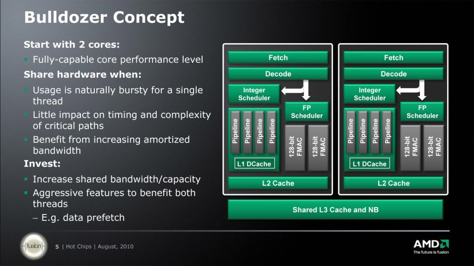
BulldozerHotChips_August24_8pmET_NDA-5_575px.jpg


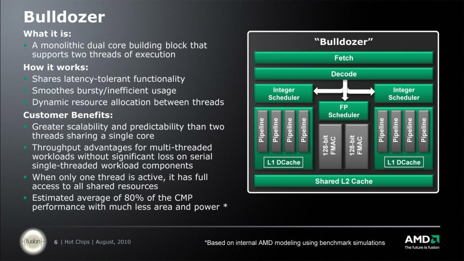
BulldozerHotChips_August24_8pmET_NDA-6_575px.jpg


But this was what they said.

I don't know if when AMD engineers started this project (and it seems it suffered several changes) they planned to changed the ratio of int:fpu from 1:1 to 2:1 or because they had a certain power usage budget and die size budget (as long as basic guideline performance) AMD decided 2 int cores could share a FPU and a few other things and then they made the changes so that could work.

Maybe they just started from barcelona cores and how to solve the performance problems.

That will be an interesting story to read.

It seems to be me we are arguing same things but just coming from different paths.

Or maybe all this comes from the following.

Of course, that's when you look at it from scratch, which is the right perspective. You see, if you start with the module being there already and you just want to add a core, you will think that it only took 12% more from the core you already had. But, if you had a module in the first place, then you already consumed more space than a normal single core. And if you already had a module but only had a single core, that means you wasted precious space (and design and engineering time) to design something for multithreaded efficiency that only had one core. It just doesn't make sense, exactly because it is the wrong perspective.

Either extra integer core and resources take a significant space or it doesn't. Maybe instead of 4 modules/8 cores a die could only have 6 cores. But maybe the space wasted on the module optimizations could have been used for getting extra performance for those cores. Maybe it could have been a core capable of HT.

So what will be better?

We will have the answer when BD is out and fighting Intel offerings
 

extra

Golden Member
Dec 18, 1999
1,947
7
81
Actually I said 3 things:
1. Interlagos will perform 50% better than MC in the same thermals
2. IPC would be higher
3. Increase for single-threaded workloads will be "a lot" more than 17%
--snip--
Based on Scali's treatment recently I just don't feel like I need to respond to him at all. Let him think whatever he wants, it is more convenient for him that way.

Thanks for posting here, we do appreciate it--don't let some of our more "obnoxious" members discourage you from posting, just ignore list them and don't reply to them, is your best bet. I learn a lot from you, Idontcare, Aigo, and a few others. Anyway.

Few questions:
1. Can you comment on that "accelerate mode" rumor that dresdenboy has posted on his blog?
2. Are you working with Microsoft, etc, to get Windows and it's associated libraries optimized to take advantage of fused multiply add? Do you anticipate it making a noticeable difference in performance? I'm not a programmer or anything, but since it's something you have that Intel doesn't (yet), I'm curious about what support you have lined up for it. Will Intel's 3 operand FMA be able to operate as a "subset" of your 4 version, or will it require completely different stuff?
3. This is a strange one...but are there any Bobcat low power server plans? :)
 

JFAMD

Senior member
May 16, 2009
565
0
0
Thanks for posting here, we do appreciate it--don't let some of our more "obnoxious" members discourage you from posting, just ignore list them and don't reply to them, is your best bet. I learn a lot from you, Idontcare, Aigo, and a few others. Anyway.

Few questions:
1. Can you comment on that "accelerate mode" rumor that dresdenboy has posted on his blog?
2. Are you working with Microsoft, etc, to get Windows and it's associated libraries optimized to take advantage of fused multiply add? Do you anticipate it making a noticeable difference in performance? I'm not a programmer or anything, but since it's something you have that Intel doesn't (yet), I'm curious about what support you have lined up for it. Will Intel's 3 operand FMA be able to operate as a "subset" of your 4 version, or will it require completely different stuff?
3. This is a strange one...but are there any Bobcat low power server plans? :)

1. No I really can't, for 2 reasons: I didn't read enough about his thoughts to know what he is referring to and the other reason is that *if* this is something in the architecture, it is not something that is disclosed yet.
2. Yes, MSFT and all of the key Linux distributions.
3. Not currently. We look at it because we need to make full use of any silicon that we have. The problem isn't the silicon, it's the market. For small servers with low utilization that just need a low power solution, virtualization does a much better job. For cloud clusters you get low power, by you seriously increase the number of physical servers, which ultimately leads to more cost and more management hassle. The market just isn't there.
 

JFAMD

Senior member
May 16, 2009
565
0
0
You are saying AMD built BD from the start as a shared dual-core or Module and they claimed that.

BulldozerHotChips_August24_8pmET_NDA-5_575px.jpg


BulldozerHotChips_August24_8pmET_NDA-6_575px.jpg


But this was what they said.

I don't know if when AMD engineers started this project (and it seems it suffered several changes) they planned to changed the ratio of int:fpu from 1:1 to 2:1 or because they had a certain power usage budget and die size budget (as long as basic guideline performance) AMD decided 2 int cores could share a FPU and a few other things and then they made the changes so that could work.

Maybe they just started from barcelona cores and how to solve the performance problems.

That will be an interesting story to read.

So, here is the story behind those slides (I actually did not make them, the engineers did, the other 95% of the server slides that you see are my team.)

This is not about showing an actual layout of bulldozer and different physical designs. This is about showing the thought process behind them.

We built the core from the ground up, we did not take an existing design and modify it. To the best of my knowledge the design was built around the sharing of components, never around seperate cores.

We were trying to show what a Bulldozer would have been like IF we had gone down the normal path that had been used in the past. The point they were making was that there was a lot of duplicated circuitry that was in the processor.

Most workloads have little or no FP,for instance. So for them, the move to 256-bit AVX would actually be a penalty. Lots more power being consumed by a big FPU that sits idle through most of the cycles. If you share a single FPU then you reduce a lot of power to the processor. That saved power budget lets you put in more integer resources, and THAT is what apps really need.

For the folks that need massive FPU, they are probably already looking at GPGPU, so the FPU in the processor is less interesting to them. The FPU in CPU is about what I would call "one off" or "random" FP and GPGPU is about large amounts of parallel FP instructions.

So those slides do not show previous concepts, what they show is bulldozer if it were implemented in the old style.

The crowd at hot chips got the full voice over, when you look at the slides only, you lose some of the context.
 

Kuzi

Senior member
Sep 16, 2007
572
0
0
Kuzi unless I am mistaken about Scali's comments I think he is right but perhaps you are mistaking the terms to mean something else that convinces you he is in error.

Anytime you have shared data domains that require coherency across threads, such as the L2$ on Q6600 which was actually split across two dual-core dies and data had to pass thru the FSB for thread access, you will see "funny business" in the thread scaling depending on the thread locality versus data locality.

This is true for Q6600 and will be true for BD. The difference with BD is the data coherency mechanism is on-die, so the effect may be negligible but we can't say, as computer scientists, that the effect will be zero. It will be a non-zero effect, perhaps immaterial but still non-zero nevertheless.

Also in regards to IPC...think about the acronym...Instructions Per Cycle. Which Instructions? Are we talking about the ability to sequentially execute the exact same instruction a few billion times a second or are we talking about some mix of instructions that represents a common application's execution pattern?

There are some 800-1000 instructions in the ISA of these modern cpus...IPC isn't really a metric we actually measure. You can, there are tools out there for measuring execution latency of each instruction in the ISA.

So let's get technical. AMD engineers the BD to have a single instruction in the ISA that is actually higher performing than its counterpart in Deneb's ISA. All the rest are 50% slower than Deneb. AMD comes out and says "IPC is faster than Deneb". Have they lied? No, there is a specific instruction in the ISA that does execute more times per cycle.

(not saying this is what AMD has done, just highlighting the absurdity of trying to rationalize IPC numbers without any info on the app used to generate the IPC comparison between architectures...and I think JF has pretty much null and voided all our speculation regarding IPC on BD above)

But it doesn't tell us what we care about...how does our app of interest perform? How much for the chip/platform? Power?

I see what you mean IDC. But you know, for a CPU core to have 2 ALUs or 3 ALUs, that's not the only determining factor for IPC. Take the Pentium 4 as an example, it had double-pumped ALUs, so if the processor frequency was 3GHz, the ALUs were running at 6GHz. Now lets read Scali's comment:

"It's virtually impossible for AMD to get more IPC out of the BD architecture, since it has less execution units per thread."

How about less execution units running at twice the speed, similar to the P4? Intel did that like 5 or 6 years ago, can AMD do it?

"Worst case, BD's pipelines will have to do 50% more work than Phenom II to reach the same throughput (two units doing the work of three). They're not going to make THAT big a jump in efficiency, that's not even remotely realistic.

Scali's comment here is inaccurate for a few reasons. First it implies that software requires all 3 ALUs every clock cycle, when in truth only 2 are needed most of the time. Also what if a BD Module was designed in such a way that it's possible to combine all 4 ALUs to decode one wide instruction?

I'm not saying DB will be able to do that, but it's still possible, especially when running 1 thread per Module. And as I mentioned above about the double-pumped ALUs, a BD core with only 2 ALUs running at 6GHz, would be 25% faster than a Phenom core running 3 ALU at 3GHz. It's all speculation of course, but it's always possible.

I would like to post a helpful comment made last year on aceshardware forums by Hans de Vries:

"I've always interpreted AMD's clustered multiprocessing, which they claimed as adding 80% performance with 50% extra transistor, as something like the following:

A 2-way superscalar processor can reach 80%-100% of the performance of a 3-way for lots of applications. Only a subset of programs really benefits from going to a 3-way. A still smaller subset benefits from going to a 4-way superscalar.

Now, if you still want to have the benefits of a 4-way core but also want to have the much higher efficiency of the 2-way cores then you can do as follows:

Design a 4-way processor which has a pipeline which can be split up into two independent 2-way pipes. In this case both threads have there own set of resources without interfering with each other.

Part of the pipeline would not be split. Wide instruction decoding would be alternating for both threads.

The split would be beneficial however for the integer units and the read/write access units to the L1 data cache. The total 4-way core could have more read/write ports which should certainly improve IPC for a substantial subset."

Hope this helps :)
 
Last edited:

Idontcare

Elite Member
Oct 10, 1999
21,118
58
91
I see what you mean IDC. But you know, for a CPU core to have 2 ALUs or 3 ALUs, that's not the only determining factor for IPC. Take the Pentium 4 as an example, it had double-pumped ALUs, so if the processor frequency was 3GHz, the ALUs were running at 6GHz. Now lets read Scali's comment:

"It's virtually impossible for AMD to get more IPC out of the BD architecture, since it has less execution units per thread."

How about less execution units running at twice the speed, similar to the P4? Intel did that like 5 or 6 years ago, can AMD do it?

Kuzi I think you might be reading Scali's comments in a manner which he did not mean to convey.

For example, some folks (most folks I suppose) view IPC as being clock-normalized.

Tell me you are double-pumping the circuit to get more work done per second and I'll agree that you are getting more work done per second, but you doubled the number of cycles that the circuit is clocking through in order to get more work done...so are you really retiring more instructions per cycle? Or did you just shift around how you count cycles (using cpu cycles instead of circuit cycles) so that your computed IPC number looks good on paper?

IPC is supposed to be clock-speed normalized. No funny business. Scali is just saying the hardware itself can only do so much per cycle, now if go and double the number of cycles then sure you are going to get more work done per second but not more work done per cycle. That is all Scali is saying as far as I can tell.

"Worst case, BD's pipelines will have to do 50% more work than Phenom II to reach the same throughput (two units doing the work of three). They're not going to make THAT big a jump in efficiency, that's not even remotely realistic.

Scali's comment here is inaccurate for a few reasons. First it implies that software requires all 3 ALUs every clock cycle, when in truth only 2 are needed most of the time. Also what if a BD Module was designed in such a way that it's possible to combine all 4 ALUs to decode one wide instruction?

Again unless I am not understanding either one of you this seems like another innocent case of misunderstanding what is being said.

Scali says "worst case" and you appear to interpret that as "best case". As I read it Scali's comment is not inaccurate, he has correctly detailed the worst-case scenario.

That there are scenarios out there that do not entail the worst-case scenario is not what he is talking about.

You both are right, near as I can tell, except for the part where you say each other are wrong, because each of you are talking about opposite ends of the same elephant.

250px-Blind_men_and_elephant3.jpg

And so these men of Hindustan
Disputed loud and long,
Each in his own opinion
Exceeding stiff and strong,
Though each was partly in the right
And all were in the wrong.
 

JFAMD

Senior member
May 16, 2009
565
0
0
Damn you and the elephant. I was halfway through my "biggest bulldozer misconceptions" blog and I started it with the elephant story. You beat me to it.
 

bryanW1995

Lifer
May 22, 2007
11,144
32
91
In specific patterns you can get over 50%:
http://www.ibm.com/developerworks/linux/library/l-htl/

no comment on the "real world" analogy?


jfamd said:
Damn you and the elephant. I was halfway through my "biggest bulldozer misconceptions" blog and I started it with the elephant story. You beat me to it.

it's 9:30 pm on a saturday, and you're the only one of us here working right now. be careful, you're going to ruin the reputation of amd marketing ;)
 
Last edited:

cbn

Lifer
Mar 27, 2009
12,968
221
106
Take the Pentium 4 as an example, it had double-pumped ALUs, so if the processor frequency was 3GHz, the ALUs were running at 6GHz.

How did this strategy fare on the energy efficiency front?
 

IntelUser2000

Elite Member
Oct 14, 2003
8,686
3,785
136
How did this strategy fare on the energy efficiency front?

The double pumped ALU couldn't execute most instructions so it didn't matter that much, performance wise.

Or did you just shift around how you count cycles (using cpu cycles instead of circuit cycles) so that your computed IPC number looks good on paper?

IDC, I think you could have just opened up a can of worms here. Though at least the comic made sense so all won't be lost in the chaos. :)
 
Last edited:

DrMrLordX

Lifer
Apr 27, 2000
21,632
10,845
136
Personally I don't think speculative threading will go anywhere any time soon. There are a lot of cool-sounding ideas out there, but there are a couple fundamental problems:
A) You're burning a tremendous amount of extra power, and we're already in a power-constrained world. You need extremely high accuracy in terms of guessing when you can safely jump ahead to be power-efficient.

I would think of it this way . . . with applications spawning more and more threads (where possible), I would think that the number of occasions during which one would want speculative threading to function would be fairly minimal. This would, ideally, be an "off and on" sort of thing that you'd only use when working with a few high-priority, resource-intensive threads under conditions that would leave a number of physical or logical cores inactive for want of threads to handle.

Done right, power consumption wouldn't necessarily go up for extended periods of time. It would take some kind of archaic, out-of-date, single-threaded number crunching app (SuperPi anyone?) to cause power-to-performance problems.

But yes, enlisting multiple cores to increase performance when handling a single thread by some relatively small amount (10%? 20%? who knows) would not make the power-to-performance ratio good, and given that fact, I do not think that you'd want to use speculative threading as a way to consistently increase IPC for a given design under most circumstances.

If you specifically wrote code with speculative multithreading in mind, it might be doable... but I don't see that happening.

It would take a good bit of leverage from whatever company introduced a particular speculative threading-capable design to get coders interested in supporting it.
 

Kuzi

Senior member
Sep 16, 2007
572
0
0
Kuzi I think you might be reading Scali's comments in a manner which he did not mean to convey.

For example, some folks (most folks I suppose) view IPC as being clock-normalized.

Tell me you are double-pumping the circuit to get more work done per second and I'll agree that you are getting more work done per second, but you doubled the number of cycles that the circuit is clocking through in order to get more work done...so are you really retiring more instructions per cycle? Or did you just shift around how you count cycles (using cpu cycles instead of circuit cycles) so that your computed IPC number looks good on paper?

You are right IDC. My thinking was if a CPU is running at 3GHz, with double-pumped ALUs at (6GHz), and we compare it against the same CPU running at 3GHz, but without the double-pumped ALUs, the first processor would end up faster. I guess I should have used the word higher "Performance" instead of higher IPC.

In the real world, when comparing those processors, we will still say it's a 3GHz CPU vs a 3GHz, even though one of them has the ALUs running at twice the frequency.

Again unless I am not understanding either one of you this seems like another innocent case of misunderstanding what is being said.

Scali says "worst case" and you appear to interpret that as "best case". As I read it Scali's comment is not inaccurate, he has correctly detailed the worst-case scenario.

That there are scenarios out there that do not entail the worst-case scenario is not what he is talking about.

Thanks for pointing that out, I'll pay more attention next time to what people type before replying. Although this worse case scenario happens very rarely, but it's still valid since it can happen.

You both are right, near as I can tell, except for the part where you say each other are wrong, because each of you are talking about opposite ends of the same elephant.

250px-Blind_men_and_elephant3.jpg

And so these men of Hindustan
Disputed loud and long,
Each in his own opinion
Exceeding stiff and strong,
Though each was partly in the right
And all were in the wrong.

Hahaha, that really made me laugh :D You hear that Scali? Stop touching the Elephant :p
 
Last edited:

AtenRa

Lifer
Feb 2, 2009
14,001
3,357
136
Very dramatic presentation, you should try it in real life.
On the other hand, we Greeks are more scientific in nature and we don’t like PR so much because you can twist the truth any way you want it.

So I will say it again one more time and I will not be concerned with this subject of the Core die area again.

You compare deferent things, a Deneb Core with a Bulldozer Core. Two Deneb cores don’t make a Bulldozer Module and two Bulldozer Modules don’t make a dual or quad Core Deneb.

If you take two Deneb cores and you take off the L2, L1, some space from the Front End and some space from the FP Unit of the second Deneb core, then yes you get almost 50% reduction for a second core DENEB.

But in Bulldozer Module, you don’t have a Single Bulldozer Core in order to make the same comparison as with Deneb cores because Bulldozer was designed as a Module from the start, meaning the Front End and the FP unit cannot be compared with a single core. We have no idea how much die area the Front End of the Bulldozer Module occupies nor for the FP unit. The only think we know is that an Integer Core occupies 12% of a Bulldozer Module, so two integer Cores only occupy 24% of the entire Module.

In a Bulldozer CPU, if you want to add a module in order to have 2 more Int cores it will take 100% more die of a single module. For example from a 4 core CPU to an 8 core CPU we need 2 more full Modules.

So when AMD says that 4 Bulldozer Int Cores only occupy 5% of the whole 4 Module Bulldozer CPU that’s true and you only need 5% more die area to install 4 more Integer Cores (That’s how AMD calls them) ) but in order to install 4 more Int Cores you need 2 more Modules, that’s the deference from PR to science. ;)

Words are cheap, facts are what matters and the fact is you cannot compare a Deneb Core with a Bulldozer Module the way you compared them.
 

GaiaHunter

Diamond Member
Jul 13, 2008
3,628
158
106
Very dramatic presentation, you should try it in real life.
On the other hand, we Greeks are more scientific in nature and we don’t like PR so much because you can twist the truth any way you want it.

So I will say it again one more time and I will not be concerned with this subject of the Core die area again.

You compare deferent things, a Deneb Core with a Bulldozer Core. Two Deneb cores don’t make a Bulldozer Module and two Bulldozer Modules don’t make a dual or quad Core Deneb.

If you take two Deneb cores and you take off the L2, L1, some space from the Front End and some space from the FP Unit of the second Deneb core, then yes you get almost 50% reduction for a second core DENEB.

But in Bulldozer Module, you don’t have a Single Bulldozer Core in order to make the same comparison as with Deneb cores because Bulldozer was designed as a Module from the start, meaning the Front End and the FP unit cannot be compared with a single core. We have no idea how much die area the Front End of the Bulldozer Module occupies nor for the FP unit. The only think we know is that an Integer Core occupies 12% of a Bulldozer Module, so two integer Cores only occupy 24% of the entire Module.

In a Bulldozer CPU, if you want to add a module in order to have 2 more Int cores it will take 100% more die of a single module. For example from a 4 core CPU to an 8 core CPU we need 2 more full Modules.

So when AMD says that 4 Bulldozer Int Cores only occupy 5% of the whole 4 Module Bulldozer CPU that’s true and you only need 5% more die area to install 4 more Integer Cores (That’s how AMD calls them) ) but in order to install 4 more Int Cores you need 2 more Modules, that’s the deference from PR to science. ;)

Words are cheap, facts are what matters and the fact is you cannot compare a Deneb Core with a Bulldozer Module the way you compared them.

Of course none of this matters either.

What matters is all those things we don't know, like price, consumption and performance.