- Apr 28, 2024
- 2,179
- 2,814
- 96
RGT: AMD likely to focus on professionals rather than gamers. Unlikely to produce an "Nvidia killer" gaming card
a) nopeAMD likely to focus on professionals rather than gamers. Unlikely to produce an "Nvidia killer" gaming card
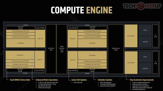
Interesting stuff. If I sum up SRAM caches of 2x CDNA4 CU (L1, LDS, Instruction Cache) I am landig at 512kB (if I am counting right). Because instructions can probably be shared -> 448kB would be the number.
RDNA4 already incorporates dynamic / out of order register allication (as M3 does). M3 then goes further and unifies its local cache, which we now might see on CDNA5 and RDNA5. But it seems, that the register files do not get merged with LDS and L0?
Edit:
Maybe it is a 512kB SRAM macro, 448kB = L1/LDS replacement and 64kByte = Dedicated Instruction Cache?

a) nope
b) final config size is relative to what NV ships by then
If they win, they win. Simple as that.I remain skeptical of AMD's ability to sell $1k+ gaming cards, regardless of competitiveness.
Bubble is dead.Chasing AI Hype makes more sense.
From C&C: https://old.chipsandcheese.com/2025/06/28/blackwell-nvidias-massive-gpu/AMD doesn't provide a lot of info. Had to go back to the CDNA 3 whitepaper + Chips and Cheese posts to find it all.
CDNA 4 CU:
CDNA 4 480kB (LDS/L1/L0) vs CDNA 5 448kB (LDS/L0) so -32kB vs CDNA 4. Do note that the CDNA 4 figure includes L1 scalar and vector cache while Kepler's only included LDS+L0.
- LDS = 160kB
- L1 vector data cache = 32kB
- L1 scalar = 16kB
- Instruction cache (shared with one CU) = 64kB/2 = 32kB
- Total: 240KB
RDNA 4 CU
RDNA 4 288KB vs RDNA5 ?,
- LDS = 64kB
- L1 vector data cache = 32kB
- L1 scalar = 16kB
- Instruction cache (shared with one CU) = 64kB/2 = 32kB
- Total: 144KB
NVIDIA Blackwell consumer SM is 128KB/SM + L0 i-cache (unknown). Compare that to 112KB L1 shared + 32KB instruction cache and now AMD is suddenly very close to where NVIDIA is rn.
In addition AMD already has a 50% larger VGPR (384kB/CU vs 256kB/SM) than NVIDIA's VRF that likely includes scalar registers as well.
Do we know how big the shared L0+LDS (maybe also L1?) is for RDNA5? There's no way it's the same size as CDNA5.
Was also wondering about that very large 512kB VGPR for CDNA and if CDNA5 makes any changes here. AMD mentioned something about a 256Kb VGPR + 256kB AGPR mode and suspect this is to match NVIDIA's Tensor memory. Tensor memory is the same size as their VRF 256KB+256KB per SM and it's also located next to VRF in SM block diagram, so it has to be a Tensor specific VRF right?
I've already tried to get @Kepler_L2 to confirm or deny this but didn't reply so suspect it's only L0/LDS but have no idea. But perhaps register file is unified so no more fixed SGPR and VGPRs, but no info disclosed on that either.
Kepler said it was shared L0/LDS, didn't mention anything about L1 scalar and vector cache, so it's prob not L0/LDS/L1.

Great, AMD going the nvidia approach and making an unobtanium halo and then the next sku down will be a fraction of the size.The Chiphell guy pretty much concurs with everything said so far, 4 dies, 2027 launch, very specifically no AT1.
oh that's baby stuff.Great, AMD going the nvidia approach and making an unobtanium halo and then the next sku down will be a fraction of the size.
Well, if it competes with a $2000 nvidia card, aren't they going to price it around that range?oh that's baby stuff.
They can build something far, far more expensive.
It would make a lot of sense if the different GPU dies can also stand alone as discrete low end graphics cards...its possible that they somehow might. UDNA= Unified DNA, but werent we just told Medusa Point was going to use RDNA 3.5 and not UDNA? Now its all UDNA?
noThere could, in theory, be Strix Halo 1.5, with the same Halo IOD but with Zen 6 CCD
Means the same thing results wise"No, it's not compatible" or "No, AMD is not likely going to release such a product"?
No means no."No, it's not compatible" or "No, AMD is not likely going to release such a product"?
To the best of my knowledge:AMD doesn't provide a lot of info. Had to go back to the CDNA 3 whitepaper + Chips and Cheese posts to find it all.
CDNA 4 CU:
CDNA 4 480kB (LDS/L1/L0) vs CDNA 5 448kB (LDS/L0) so -32kB vs CDNA 4. Do note that the CDNA 4 figure includes L1 scalar and vector cache while Kepler's only included LDS+L0.
- LDS = 160kB
- L1 vector data cache = 32kB
- L1 scalar = 16kB
- Instruction cache (shared with one CU) = 64kB/2 = 32kB
- Total: 240KB
RDNA 4 CU
RDNA 4 288KB vs RDNA5 ?,
- LDS = 64kB
- L1 vector data cache = 32kB
- L1 scalar = 16kB
- Instruction cache (shared with one CU) = 64kB/2 = 32kB
- Total: 144KB
NVIDIA Blackwell consumer SM is 128KB/SM + L0 i-cache (unknown). Compare that to 112KB L1 shared + 32KB instruction cache and now AMD is suddenly very close to where NVIDIA is rn.
In addition AMD already has a 50% larger VGPR (384kB/CU vs 256kB/SM) than NVIDIA's VRF that likely includes scalar registers as well.
Do we know how big the shared L0+LDS (maybe also L1?) is for RDNA5? There's no way it's the same size as CDNA5.
Was also wondering about that very large 512kB VGPR for CDNA and if CDNA5 makes any changes here. AMD mentioned something about a 256Kb VGPR + 256kB AGPR mode and suspect this is to match NVIDIA's Tensor memory. Tensor memory is the same size as their VRF 256KB+256KB per SM and it's also located next to VRF in SM block diagram, so it has to be a Tensor specific VRF right?
I've already tried to get @Kepler_L2 to confirm or deny this but didn't reply so suspect it's only L0/LDS but have no idea. But perhaps register file is unified so no more fixed SGPR and VGPRs, but no info disclosed on that either.
Kepler said it was shared L0/LDS, didn't mention anything about L1 scalar and vector cache, so it's prob not L0/LDS/L1.

Inb4 wccftech yoinks this and makes a 4 paragraph article on it.To the best of my knowledge:
View attachment 129324
Does this look right? I'm sure I have some mistakes, so let me know where I should make adjustments. I can also add rows for # of executions units as well, etc.To the best of my knowledge:
View attachment 129324

Then each of those UMC blocks in @Kepler_L2 's diagrams are 2*16bit LPDDR5 and not just 16bit? Otherwise it'll be bandwidth starved.I think the M in 'GMD' stands for 'memory'.
I.e. all the DDR shoreline is there.
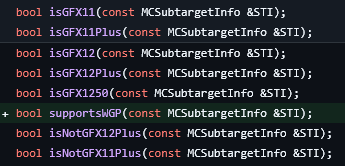
Are there any leaked arch docs/drivers which indicate which way AMD is going with RDNA 5 on wgp vs cu ?In his latest video about leaking the PS6 handheld, MLID claims the RDNA5 CUs are not RDNA4 WGP-equivalent.
Not directly but you can read between the linesAre there any leaked arch docs/drivers which indicate which way AMD is going with RDNA 5 on wgp vs cu ?


Then there's the anomaly Navi33. Know it's N6 but that can't explain +39.6% Mtr/mm^3.That is for a 128 bit bus. 256bit with 2GB chips supports 16GB as standard or 32GB with clamshell.
251mm for N10. 237mm for N23. It is not that much of a saving.
Yep. See belowI think the M in 'GMD' stands for 'memory'.
I.e. all the DDR shoreline is there.
GMD = Graphics Memory Die
RDNA1-4 has no WGP/CU level caches higher than L0. L1 is located in the Shader Arrays (two per SE). CDNA kept some GCN baggage.Does this look right? I'm sure I have some mistakes, so let me know where I should make adjustments. I can also add rows for # of executions units as well, etc.
View attachment 129328

Then each of those UMC blocks in @Kepler_L2 's diagrams are 2*16bit LPDDR5 and not just 16bit? Otherwise it'll be bandwidth starved.
Maybe CDNA 6? MI500 !?@Kepler_L2 is CDNA5 a clean slate µarch like RDNA5?


