Discussion RDNA 5 / UDNA (CDNA Next) speculation

Page 48 - Seeking answers? Join the AnandTech community: where nearly half-a-million members share solutions and discuss the latest tech.

adroc_thurston

Diamond Member
Jul 2, 2023
7,102
9,859
106
Fermi has L1/shared memory, uniform cache, and texture cache. NVIDIA Volta merged texture cache and L1/shared memory into one big shared cache.
Nope.
GF100 is no different from GV100 caching-wise.
L0 in RDNA4 is literally texture cache (check the RDNA4 WGP diagram)
All first-level shader-core private caches are inherently texture caches.
while LDS is equivalent to L1/shared
Nope, LDS is LDS.
It's the scratchpad that's been with us since Terascale1.
GFX12.5 merges this aligning with Volta
Nope.
They do it their own way.
and as Kepler has established through LLVM GFX13 will do the same.
oh no my friend.
 

MrMPFR

Member
Aug 9, 2025
103
207
71
Nope.
GF100 is no different from GV100 caching-wise.

All first-level shader-core private caches are inherently texture caches.

Nope, LDS is LDS.
It's the scratchpad that's been with us since Terascale1.

Nope.
They do it their own way.

oh no my friend.

Really just ignore this entire post and skip to #1,201. Read adroc's replies if you like.

This is demonstrably false. Maybe not on a physical level but the cache programming model has increased flexibility and that's only possible with HW changes to the underlying data cache.

You can check the Anandtech GF100 coverage: https://web.archive.org/web/20250409030607/https://www.anandtech.com/show/2918/2
And compare it with TPU's 2080 ti review:

Reiterating GF100 = Texture cache + uniform cache + L1/shared memory while TU102 = L1 data cache/shared memory. This is misleading.

IDK about that, but the L0 matches the functionality of the Texture cache in Pre-Volta. Directly coupled to TMUs like NVIDIA's TEX units (not sure what the name is). Like that cache it's fixed and can't be repurposed. This is once again misleading. The Volta tuning guide (included in #1,201) mentions no change to the Texture cache. Mentions texture/L1 is kept from Pascal but then only L1 gets a size increase, so no AMD's implement will not be identical to NVIDIA's aligning with what Adroc said. Also there's no physical cache that can only be a texture cache, there's one shared data cache and a corresponding cache programming model for each gen that decides what the GPU can do with that cache. Skip ahead to find out more.

Roughly equivalent, not 100%.
K cache + instruction cache = private SIMD partition L0-i caches
LDS = L1/shared memory
L0 = Texture cache

Very misleading. NVIDIA's cache hierarchy is very different from AMD's GCN implementation. RDNA didn't really break the mold here, only build upon what was already there.

Besides esoteric differences L0+LDS unification is similar to Texture cache + L1/shared unification. It merges all on die caches that're not instruction caches into one big pool. Misleading so once again skip ahead or read the Volta tuning guide section on unified memory.

Commenting on NVIDIA's RTX Hair technology on X, tech-savvy user LeviathanGamer posted a list of tech they think would vastly improve ray tracing performance, including
fast Matrix Math, for which RDNA4 architecture laid a lot of groundwork,
  1. 2x Intersection Testing,
  2. unified LDS/L0 Cache,
  3. Dedicated Stack Management and Traversal HW,
  4. Coherency Sorting HW, and
  5. 3-coordinate decompression Geometry HW.

Commenting on this list, well-known AMD leaker Kepler L2 said on the NeoGAF forums that the next AMD GPU architecture that will power the PlayStation 6 and next-generation Xbox will have all this tech, and a lot more,


@Kepler_L2's comment leaves no room for discussion. RDNA5 will have CDNA5's LDS/L0. Wrong. LLVM code only was about one feature level: flexible LDS+L0 vs GCN and RDNA's rigid LDS and L0. There will probably be additional overhauls to the HW that enables a radically different cache system. Adroc keeps reapeating this and Kepler doesn't correct this. Would be disappointing if it weren't true when CDNA5 is GFX12.5 < GFX13 (RDNA5). GFX12.5 implies no GCN baggage and improved upon RDNA4 that strips out all the gaming stuff, whereas GFX13 implies something completely new.
 
Last edited:

adroc_thurston

Diamond Member
Jul 2, 2023
7,102
9,859
106
This is demonstrably false.
It's true.
tex caches became dcaches to accomodate compute shading/GPGPU apps.
Reiterating GF100 = Texture cache + uniform cache + L1/shared memory while TU102 = L1 data cache/shared memory.

IDK about that, but the L0 matches the functionality of the Texture cache in Pre-Volta. Directly coupled to TMUs like NVIDIA's TEX units (not sure what the name is). Like that cache it's fixed and can't be repurposed.

Roughly equivalent, not 100%.
K cache + instruction cache = private SIMD partition L0-i caches
LDS = L1/shared memory
L0 = Texture cache
please stop arguing with me it's plain stupid.
It merges all on die caches that're not instruction caches into one big pool.
See in AMD case it's much weirder than that.
RDNA5 will have CDNA5's LDS/L0.
different.
 

soresu

Diamond Member
Dec 19, 2014
4,105
3,566
136
At least until something like Asus BTF comes up as a standard
BTF is just an Asus marketing thing for the whole "invisible cabling" platform.

GC_HPWR is the ultra high power connector in question, but in reality it's only pushing the ball down the road to the motherboard instead of the GPU - because that power still has to come from somewhere.

It does seem like non Asus mobo/gfx AIB manufacturers (Sapphire at least) are up for it, but it's anyones guess as to whether that will lead to a change in ATX to support it.
 

adroc_thurston

Diamond Member
Jul 2, 2023
7,102
9,859
106
BTF is just an Asus marketing thing for the whole "invisible cabling" platform.

GC_HPWR is the ultra high power connector in question, but in reality it's only pushing the ball down the road to the motherboard instead of the GPU - because that power still has to come from somewhere.

It does seem like non Asus mobo/gfx AIB manufacturers (Sapphire at least) are up for it, but it's anyones guess as to whether that will lead to a change in ATX to support it.
We just need to uhhhhh kill ATX
 

soresu

Diamond Member
Dec 19, 2014
4,105
3,566
136
We just need to uhhhhh kill ATX
Not the worst idea.

It desperately needs to change so that the DIMM slots are rotated 90 degrees allowing a clean (or at least minimal impedance) airflow from rear case fan -> CPU cooler -> DIMM slots -> front case fans.

ATX clearly wasn't designed with air flow in mind.
 

MrMPFR

Member
Aug 9, 2025
103
207
71
They could probably even aim at 64x XBSX streams with such a system:
- 8x AT0 cards with 184 CU at ~2.7 GHz deliver ~1000 TFLOPS => 82x XBSX
- 2S Venice could feature 2*256C = 512C => 64x XBSX
Remember that one RDNA5 CU is a lot stronger than RDNA2 CU. Xbox will prob market it >100 XSX is one server blade.
With the IPC gains maybe they could get away with using lesser config. 2 x 192C should be more than enough especially with the absurd clocks on N2P in 2027+.

The push towards RTRT or especially HWRT will change with the next console cycle. Not because RTRT drives graphics forward, which RTRT definitely will, but because it will change production pipelines of games.
No more or at least vastly reduced baking, shortened development cycles. RTRT is mainly a game changer for developers. Not for gamers. But we as gamers might get better or, to be more precisely, more consistent quality. Because HWRT gets rid of the biggest illumination flaws of raster approximations.

PS5 etc. as last-gen consoles feature HWRT in a good enough fashion to make that shift. You can see it live happening if looking at UE5 development processes. SW-Lumen got frozen since UE 5.4 or 5.5, no further development.
MegaLights should scale from PS5, Switch 2 etc. up to PS6 and eventually Highend-PC. Replacing SW and HW Lumen as it is available today. Read the MegaLights presentation of Epic at Siggraph 2025: https://advances.realtimerendering.com/s2025/content/MegaLights_Stochastic_Direct_Lighting_2025.pdf
And MegaLights must scale that widely. Why? Because you do not want to design a game with hundreds of light sources and then scale down to a PS5 without MegaLights. That will not work.

HWRT together with a very scalable RTGI solution like MegaLights with virtually no limits on light source count will be the future. Starting with PS6 and Xbox-Next release. Main reason: Game development.
In that regard, RTXDI from Nvidia based on ReSTIR is conceptually the very same thing as MegaLights. Just geared towards the upper end of the quality spectrum (and HW requirements).

Regarding PC costumers, HWRT or RTRT will not really drive buying decisions too much, because the hardware is already here today. It is more about general performance of your card.
RDNA4 supports good HWRT and Nvidia cards since ages (if featuring enough VRAM). I expect the gap to be closing even further with RDNA5.
And when the next console cycle begins, not too many PC users will own a card with bad RT acceleration (Nvidias market share is too big to be otherwise).
RDNA2 and RDNA3 cards might struggle, I don't know. But if techniques like MegaLights run on a PS5, it should also run on a 6700XT at similar quality settings.

Agree with @adroc_thurston here. MLPs will supplant RT mostly or completely. AMD LSNIF already tries to replace BLAS entirely with neural representation, there's neural radiance caching, NVIDIA neural materials, NVIDIA NRC to extend ReSTIR well beyond realtime fidelity, Intel translucency MLP, NVIA going the same route, what's next. IDK but what NVIDIA showed at CES is only the beginning.
Even further out NeRFs and neural gaussian splits will make things even wilder.

So HWRT will become much less relevant, not for the crossgen era, but beyond that things will change massively. The question is how long will crossgen be. Every day it seems like SWEs breathe new life into current gen consoles so suspect crossgen will be VERY long nextgen. But even for crossgen period wouldn't be surprised if we see increasingly larger portions of the rendering on PS6 being offloaded to ML HW.

There's no way Megalights will be able to run on a Switch 2, even XSS is a stretch.

Nice another person who saw the Megalights UE5 PDF from SIGGRAPH. It's amazing they're creating what will essentially be an optimized ReSTIR (not quite as good) that runs on the anemic RT cores of the PS5 and XSX. That's the last thing I thought would happen.
Remember Cerny in the DF PS5 Pro exclusive interview talking about PT on PS5 Pro being unlikely but wouldn't discount what devs could do. The PS5 Pro will def run a proper full version that leverages RTX Mega geometry like BVH functionality for proper detail for direct lighting but still well below desktop ReSTIR implementation (too demanding).

Yeah RDNA2-3 is probably doable for as long as PS5 and XSX are supported.
 

MrMPFR

Member
Aug 9, 2025
103
207
71
It's true.
tex caches became dcaches to accomodate compute shading/GPGPU apps.

please stop arguing with me it's plain stupid.

See in AMD case it's much weirder than that.

different.

Think we're talking past each other.
I was refering to the HW level implementation (SRAM stores) and how the cache pools in pre-Volta are fixed, that's they can only do one one or a few things. In Fermi there's a fixed SRAM store for Texture cache/dcache, uniform cache (IDK what this is for,) L1 cache/shared memory, and instruction cache (ignore this for now).
L1/shared memory SRAM store absent from Maxwell and Pascal SM where they moved to a L1/texture cache/dcache x 2 and one shared cache.

You're 100% right that the way the shared cache block in Volta and later gets partitioned and functions when exposed to SW is unchanged from Fermi. Only change is the added flexibility (ratios) betwen stores that's possible by having one SRAM store exposed to SW instead of multiple stores small less flexible or completely inflexible as explained in the Turing whitepaper quoted by me.
This is extremely misleading. SW programming model is an abstraction of the actual HW as indicated in the Volta tuning guide that I included in #1,201. The SM block diagram is not about the physical SRAM stores but how a shared datacache is used and how flexible it is via the programming mode (HW meets SW).
Also saw AMD calling their equivalent L0 a vector cache in C&Cs RDNA3 article so yeah seems like it's multipurpose across vendors. Not surprising since GCN was also GPGPU focused and RDNA3 is an extension of that. This is misleading. Since Maxwell NVIDIA merged the L1 and texture cache into one function somehow (Read the Volta tuning guide). Also we don't know the intricacies of the HW implementation, all you need to know is that AMD's WGP cache system is less flexible than the one found in NVIDIA Volta and later.

Seems like NVIDIA DC has kept the big L1 instruction cache while consumer only gets private L0-i caches within each SM so yeah AMD's implementation is not aligned with NVIDIA's on a HW level. We can't know for sure here's it's possible AMD has tiny instruction caches in each SIMD unit (four in a WGP) that they didn't bother to mention.

Do you have insider info? Because I haven't heard @Kepler_L2 say anything other than 2 x L0 slabs and LDS gets unified into one big slab exposed to different ratios via SW in CDNA5/GFX12.5.
This is incredibly embarrasing. GFX12.5 implies RDNA4 roots (obviously no gaming stuff), while GFX13 implies something entirely different. Both might share the same feature but that doesn't mean they're the same. It's like saying because both cards can do RT, the new card won't be able to do it in ways that expand upon the lastgen spec.

Again would like to know how GFX13 cache memory setup on a HW level is different from GFX12.5?
Kinda says it in the name right? See prev comment. One is based on RDNA4 (GFX12.5 vs GFX12, all prev CDNA was GFX9.x (Vega derived)) while the other (GFX13) architecture that according to Kepler is the biggest change since GCN.

Edit: I know LDS and L1/shared memory isn't the same in terms of how the µarch interfaces with them, but on HW level (SRAM blocks) they're pretty much identical in terms of being SRAM blocks for similar caches:

#1 (texture/data cache): L0 vector cache = Texture cache/data cache.
#2: (instruction caches) Instruction cache = K cache + scalar cache - in Turing and later this is moving into SIMD partitions.
#3 (shared local caches and other): LDS = L1/shared memory (Fermi functionality), as for Pascal/Maxwell no this isn't the same as I explained above, here I was wrong.
This is just flat out wrong. Skip ahead.
 
Last edited:

MrMPFR

Member
Aug 9, 2025
103
207
71
words words words completely disconnected from reality.
congrats.

Did you read the PDF? Except the made for nexgen console claim (MegaLights made for PS5/PS6 crossgen era) that's what the lead SWEs behind UE5's MegaLights are saying.
Claim MegaLights is a scaled down version that roughly matches the functionality of NVIDIA ReSTIR PT targeting.
 

adroc_thurston

Diamond Member
Jul 2, 2023
7,102
9,859
106
and how the cache pools in pre-Volta are fixed
They aren't.
In Fermi there's a fixed SRAM store for Texture cache/dcache, uniform cache (IDK what this is for,) L1 cache/shared memory, and instruction cache (ignore this for now).
It's L1/shmem slab for L1d, tex and shmem, plus icaches.
Uniform caches lasted for a while, until Hopper IIRC.
You're 100% right that the way the shared cache block in Volta and later gets partitioned and functions when exposed to SW is unchanged from Fermi. Only change is the added flexibility (ratios) betwen stores that's possible by having one SRAM store exposed to SW instead of multiple stores small less flexible or completely inflexible as explained in the Turing whitepaper quoted by me.
no it's the same. Kepler was also the same.
Seems like NVIDIA DC has kept the big L1 instruction cache while consumer only gets private L0-i caches within each SM so yeah AMD's implementation is not aligned with NVIDIA's on a HW level.
No, they all have a tiny L0i for each warp scheduler.
Then you have L1i on top of that for each SM.
Again would like to know how GFX13 cache memory setup on a HW level is different from GFX12.5?
it's weird. that's all you gotta know.
 

branch_suggestion

Senior member
Aug 4, 2023
826
1,805
106
They could probably even aim at 64x XBSX streams with such a system:
- 8x AT0 cards with 184 CU at ~2.7 GHz deliver ~1000 TFLOPS => 82x XBSX
- 2S Venice could feature 2*256C = 512C => 64x XBSX
Yeah I was being conservative.
At most you can do 64x streams of roughly XSX quality with 1SE/64b GDDR7 per stream, could be up to 16GB.
Rough estimate is >2x server PPW and >6x server density.
For the higher quality tier you can do 16x streams with similar or higher quality to the new console.
My guess is they will probably run each card at 450W max to be in the optimal part of the curve.
 
  • Like
Reactions: basix

ToTTenTranz

Senior member
Feb 4, 2021
686
1,147
136
Not the worst idea.

It desperately needs to change so that the DIMM slots are rotated 90 degrees allowing a clean (or at least minimal impedance) airflow from rear case fan -> CPU cooler -> DIMM slots -> front case fans.

ATX clearly wasn't designed with air flow in mind.
CPUs were 10 to 15W when ATX was introduced, and GPUs were even less.

Intel did try to introduce BTX 10 years later when Pentium 4 started pushing towards 75W, but ATX was too entrenched by that time.

To be honest, I too think the x86 market is bound for a massive overhaul. 4U servers can get 8x fanless >300W GPUs in a row but desktops versions need 2Kg of copper and 3 large fans each because everything is just in the way of proper airflow.
 

basix

Senior member
Oct 4, 2024
250
505
96
Wrong because we're gonna be doing even less RTRT than we do now, replacing it with ML approximations.

words words words completely disconnected from reality.
congrats.
What is your reality then? ML/AI everything in games? On what hardware? On PS6 and losing PS5 user base because of lacking HW acceleration?

I am not sure who is more disconnected from reality (note: you are the one who always proclaims the AI bubble bursting). Reality means money & business and business means having a wide spread user base.

Today, you can augment RTRT or rendering in general with ML/AI, absolutely. DLSS and Ray Reconstruction are perfect examples for that.
But that does not invalidate my argument, that RTRT is the future of game development and will get a push with next gen consoles. The core is still RTRT.
Anything which goes further than that (extensive or even pure use of ML in games) is very far in the future and not really happening before the next-next console cycle (as we have seen with RTRT on current gen consoles).

And maybe another point for you:
Even without a single ray being traced in a scene and all being replaced by ML approximations, it will still be mimicking RTRT.
Same result regarding game development pipeline and gaming experience. It is just RTRT implemented with different tools. Maybe we should define what "RTRT" means before calling each other out ;)
But as I said, current gen consoles will have big troubles with too much ML/AI in games. So we will see some ML baby steps until the next-next console cycle arrives and a true ML revolution will take place.

Did you read the PDF? Except the made for nexgen console claim (MegaLights made for PS5/PS6 crossgen era) that's what the lead SWEs behind UE5's MegaLights are saying.
Claim MegaLights is a scaled down version that roughly matches the functionality of NVIDIA ReSTIR PT targeting.
Thanks, at least one person reads stuff and gains some insights :)

Edit:
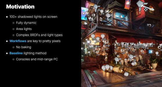
You do not even have to read that much of the PDF to find the main motivations behind MegaLights (page 2 is enough):
- Simplified, unified and better workflows for developers
- MegaLights as baseline lighting method for all target systems (HWRT based)
megalights_motivation.JPG
 
Last edited:
  • Like
Reactions: Kryohi and MrMPFR

MrMPFR

Member
Aug 9, 2025
103
207
71
They aren't.

It's L1/shmem slab for L1d, tex and shmem, plus icaches.
Uniform caches lasted for a while, until Hopper IIRC.

no it's the same. Kepler was also the same.

No, they all have a tiny L0i for each warp scheduler.
Then you have L1i on top of that for each SM.

it's weird. that's all you gotta know.

Man this entire post is a mess and I removed the SM diagrams because they cluttered the feed and are misleading. They're easy to look up on the web. Just skip to #1,201.

Here the short version. The Volta tuning guide explains what you need to know. Entire cache system mentioned here is backed by a shared data cache. Volta didn't change this it only made it more flexible and this is pretty much how things are unchanged on consumer side up until now. The shared cache is flexible and has been flexible since IDK when. Only change with Volta is added flexibility in the L1 cache that can now grow much bigger and a change to the Shared cache that's explained in the Volta tuning guide.


Then how an they state this in the official NVIDIA Turing whitepaper? https://images.nvidia.com/aem-dam/e...ure/NVIDIA-Turing-Architecture-Whitepaper.pdf

"Second, the SM memory path has been redesigned to unify shared memory, texture caching, and memory load caching into one unit. This translates to 2x more bandwidth and more than 2x more capacity available for L1 cache for common workloads."
- It's a memory path, not a cache. Skip to my next comment.

"Turing’s SM also introduces a new unified architecture for shared memory, L1, and texture caching. This unified design allows the L1 cache to leverage resources, increasing its hit bandwidth by 2x per TPC compared to Pascal, and allows it to be reconfigured to grow larger when shared memory allocations are not using all the shared memory capacity. The Turing L1 can be as large as 64 KB in size, combined with a 32 KB per SM shared memory allocation, or it can reduce to 32 KB, allowing 64 KB of allocation to be used for shared memory. Turing’s L2 cache capacity has also been increased"
- Already explained this above. Skip as ^

"Figure 6 shows how the new combined L1 data cache and shared memory subsystem of the Turing SM significantly improves performance while also simplifying programming and reducing the tuning required to attain at or near-peak application performance. Combining the L1 data cache with the shared memory reduces latency and provides higher bandwidth than the L1 cache implementation used previously in Pascal GPUs."
- Programming model derived abstraction and not the physical HW implementation. It's about memory paths not caches.


The SM block diagram in the Anandtech 2010 article disagrees.
Removed this to declutter thread.

Again how do you then explain this SM diagram + the quotes from the Turing whitepaper?
Removed to declutter thread.

Interesting. Does this carry over to Ada Lovelace and Blackwell client or only DC?

L1i + Instruction buffer (they didn't call this L0-i. See quote below) for each warp scheduler in Pascal+Maxwell consumer and for later DC it's always L1-i + L0-i. Consumer only has L0-i cache in SM diagram for Turing and later. Notice this quote from official NVIDIA blog that omits L1-i entirely: https://developer.nvidia.com/blog/nvidia-turing-architecture-in-depth/ Disputed but an odd discrepancy as highlighted in #1,201.

"The Turing SM is partitioned into four processing blocks, each with 16 FP32 Cores, 16 INT32 Cores, two Tensor Cores, one warp scheduler, and one dispatch unit. Each block includes a new L0 instruction cache and a 64 KB register file. The four processing blocks share a combined 96 KB L1 data cache/shared memory. Traditional graphics workloads partition the 96 KB L1/shared memory as 64 KB of dedicated graphics shader RAM and 32 KB for texture cache and register file spill area. Compute workloads can divide the 96 KB into 32 KB shared memory and 64 KB L1 cache, or 64 KB shared memory and 32 KB L1 cache."


Turing vs Pascal SM:
Ada Lovelace SM. There's still no L1-i.

Again misleading. Pictures removed to declutter thread.

I see so neither you or @Kepler_L2 are willing to spill the beans on GFX13's >CDNA5 cachemem changes. Guess we'll just have to wait until it becomes exposed in the LLVM compiler. Yes. Changes because GFX12.5 is RDNA4 derived in some form (current and prev CDNA has been GFX9.x for four gens so Vega derived) while GFX13 is a clean slate and the largest redesign since GCN according to Kepler.
 
Last edited:

adroc_thurston

Diamond Member
Jul 2, 2023
7,102
9,859
106
Then how an they state this in the official NVIDIA Turing whitepaper? https://images.nvidia.com/aem-dam/e...ure/NVIDIA-Turing-Architecture-Whitepaper.pdf

"Second, the SM memory path has been redesigned to unify shared memory, texture caching, and memory load caching into one unit. This translates to 2x more bandwidth and more than 2x more capacity available for L1 cache for common workloads."

"Turing’s SM also introduces a new unified architecture for shared memory, L1, and texture caching. This unified design allows the L1 cache to leverage resources, increasing its hit bandwidth by 2x per TPC compared to Pascal, and allows it to be reconfigured to grow larger when shared memory allocations are not using all the shared memory capacity. The Turing L1 can be as large as 64 KB in size, combined with a 32 KB per SM shared memory allocation, or it can reduce to 32 KB, allowing 64 KB of allocation to be used for shared memory. Turing’s L2 cache capacity has also been increased"

"Figure 6 shows how the new combined L1 data cache and shared memory subsystem of the Turing SM significantly improves performance while also simplifying programming and reducing the tuning required to attain at or near-peak application performance. Combining the L1 data cache with the shared memory reduces latency and provides higher bandwidth than the L1 cache implementation used previously in Pascal GPUs."


The SM block diagram in the Anandtech 2010 article disagrees.

View attachment 129523

Again how do you then explain this SM diagram + the quotes from the Turing whitepaper?

Interesting. Does this carry over to Ada Lovelace and Blackwell client or only DC?

L1i + Instruction buffer (they didn't call this L0-i. See quote below) for each warp scheduler in Pascal+Maxwell consumer and for later DC it's always L1-i + L0-i. Consumer only has L0-i cache in SM diagram for Turing and later. Notice this quote from official NVIDIA blog that omits L1-i entirely: https://developer.nvidia.com/blog/nvidia-turing-architecture-in-depth/

"The Turing SM is partitioned into four processing blocks, each with 16 FP32 Cores, 16 INT32 Cores, two Tensor Cores, one warp scheduler, and one dispatch unit. Each block includes a new L0 instruction cache and a 64 KB register file. The four processing blocks share a combined 96 KB L1 data cache/shared memory. Traditional graphics workloads partition the 96 KB L1/shared memory as 64 KB of dedicated graphics shader RAM and 32 KB for texture cache and register file spill area. Compute workloads can divide the 96 KB into 32 KB shared memory and 64 KB L1 cache, or 64 KB shared memory and 32 KB L1 cache."

Turing vs Pascal SM:
View attachment 129524

Ada Lovelace SM. There's still no L1-i.
View attachment 129525

I see so neither you or @Kepler_L2 are willing to spill the beans on GFX13's >CDNA5 cachemem changes. Guess we'll just have to wait until it becomes exposed in the LLVM compiler.
oh my god you're going by the NV marketing blurbs.
it's over
 

soresu

Diamond Member
Dec 19, 2014
4,105
3,566
136
CPUs were 10 to 15W when ATX was introduced, and GPUs were even less.
Did GPUs even have AIBs back then?

I seem to remember my dad or my uncle having to upgrade a computer to a Cirrus Logic GPU for Duke Nukem 3D perhaps, but I don't remember an AIB.

It would be amazing if the Vaire pseudo reverse computing (energy harvesting/reuse) tech actually works and reduces consumer compute TDPs back to 90s levels.

Having a halfway decent desk PC that is actually as thin as a desk rather than tower THICC like Lian Li's desk case range would be amazing.
 
Last edited:

soresu

Diamond Member
Dec 19, 2014
4,105
3,566
136
AGP existed for a reason.
I'm talking pre AGP, we had computers in my house years before that.

My own first computer definitely didn't have it as AGP wasn't introduced until a year later.

Looking up ATX it preceded AGP by 2 years also.
 

ToTTenTranz

Senior member
Feb 4, 2021
686
1,147
136
Did GPUs even have AIBs back then?

I seem to remember my dad or my uncle having to upgrade a computer to a Cirrus Logic GPU for Duke Nukem 3D perhaps, but I don't remember an AIB.

It would be amazing if the Vaire pseudo reverse computing (energy harvesting/reuse) tech actually works and reduces consumer compute TDPs back to 90s levels.

Having a halfway decent desk PC that is actually as thin as a desk rather than tower THICC like Lian Li's desk case range would be amazing.
The GPU term was only coined by Nvidia after it introduced the first GeForce 256 with Transform and Lighting acceleration, but that was only in 99.
The first consumer 3D accelerators came from 3dfx and PowerVR in 96 or something. Those you still had to connect to a 2D graphics card like the super popular S3 Virge because they didn't have that function.

Back when I got my first graphics card, the Voodoo 2 in 98, there were two OEMs selling voodoo cards in my country: Diamond and Creative.
 

ToTTenTranz

Senior member
Feb 4, 2021
686
1,147
136
#name I have not heard in long time

Creative actually got bigger after they left the GPU market after the Geforce 4 and focused on sound cards using their proprietary EAX sound processors. But shortly after that Microsoft blocked external sound APIs from DirectX in games, so for the past 2 decades they've been steadily but very slowly withering away. I think their founder died last year.
IMO they still make excellent sound products with great value. I use their Aurvana Ace 2 as my daily IEMs and they're pretty awesome. I still used their Gigaworks S750 7.1 in my desktop PC until a couple weeks ago (got tired of all the wiring and some of the speaker opamps finally started giving away after >20 years).


Diamond got sold to S3, and then S3 got sold to VIA, which was sold to HTC, and now somehow the brand belongs to TUL (Powercolor & Sparkle). I guess part of me wants to believe some of Diamond's engineers are now still designing graphics cards.
 
  • Like
Reactions: DAPUNISHER