
- Nov 27, 2007
- 2,044
- 5,103
- 136
Saw a really interesting article about packaging on wikichip yesterday:
 fuse.wikichip.org
It discusses a new vendor agnostic interface of doing Multi-Chip Modules, like what AMD is doing currently with Zen2. That is without silicon-on-silicon expensive stuff like Interposers and silicon bridges.
It seems that MCM can be much further than I imagined, Here is a comparison to other technologies (including the one currently used in Zen). I suggest to read the entire article but the most interesting part was probably this table:

OCP has a working prototype on GlobalFoundries 14nm process, they say that on TSMC 7nm power should be down to 0.5pJ/bit. Compared to Zen that's a 3x increase in peak data rate at nearly 4x less power per-pin.
Another really interesting part was this:
Intel get's ~40ns with 9900K with highest-end tight timings while it's ~55ns at stock (2666 Mhz). Zen 3 doesn't really go below 60ns even with the most aggressive timings and on cheaper 3200Mhz/3600Mhz RAM ~70nm is common. So taking Skylake as reference 45-50ns memory latency on a future Zen architecture should be theoretically doable.
As the technology is still in the prototype phase, Zen 3 taped out last year and AMD is only an opencompute community member (compared to say Intel that is Platinum), I doubt we'll see anything like that used in Zen 3 (though one could hope). Still there is significant performance sitting on the table even for MCP.
TL;DR:
(e.g. what was new to me)
1. MCM processors without fancy interposers/2.5D solutions still have a lot of juice left compared to what AMD has currently implemented with Zen 2.
2. Good MCM design has a smaller impact on memory latency than people think. Even with chiplets 45-50ns should be perfectly doable.
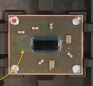
OCP Bunch of Wires: A New Open Chiplets Interface For Organic Substrates
A look at a Bunch of Wires, a new open standard chiplets interconnect being proposed by the OCP ODSA group intended for standard organic multi-chip packages as a cheaper alternative to silicon interposers and bridges.
It discusses a new vendor agnostic interface of doing Multi-Chip Modules, like what AMD is doing currently with Zen2. That is without silicon-on-silicon expensive stuff like Interposers and silicon bridges.
It seems that MCM can be much further than I imagined, Here is a comparison to other technologies (including the one currently used in Zen). I suggest to read the entire article but the most interesting part was probably this table:
OCP has a working prototype on GlobalFoundries 14nm process, they say that on TSMC 7nm power should be down to 0.5pJ/bit. Compared to Zen that's a 3x increase in peak data rate at nearly 4x less power per-pin.
Another really interesting part was this:
Which goes to show, that chiplet-design in itself shouldn't add that much latency (something th at chiakokhua has also estimated on twitter). Using chiplets should only add ~5ns to memory latency.Since dies are spaced apart, a trace length of 25mm to 50mm is required with a latency of sub-5ns
Intel get's ~40ns with 9900K with highest-end tight timings while it's ~55ns at stock (2666 Mhz). Zen 3 doesn't really go below 60ns even with the most aggressive timings and on cheaper 3200Mhz/3600Mhz RAM ~70nm is common. So taking Skylake as reference 45-50ns memory latency on a future Zen architecture should be theoretically doable.
As the technology is still in the prototype phase, Zen 3 taped out last year and AMD is only an opencompute community member (compared to say Intel that is Platinum), I doubt we'll see anything like that used in Zen 3 (though one could hope). Still there is significant performance sitting on the table even for MCP.
TL;DR:
(e.g. what was new to me)
1. MCM processors without fancy interposers/2.5D solutions still have a lot of juice left compared to what AMD has currently implemented with Zen 2.
2. Good MCM design has a smaller impact on memory latency than people think. Even with chiplets 45-50ns should be perfectly doable.
