NVidia announces Carmel ARM CPU

NTMBK

Lifer
Nov 14, 2011
10,208
4,940
136
DS_kVyxV4AA_CLi.jpg


https://twitter.com/PatrickMoorhead/status/950229121233137664

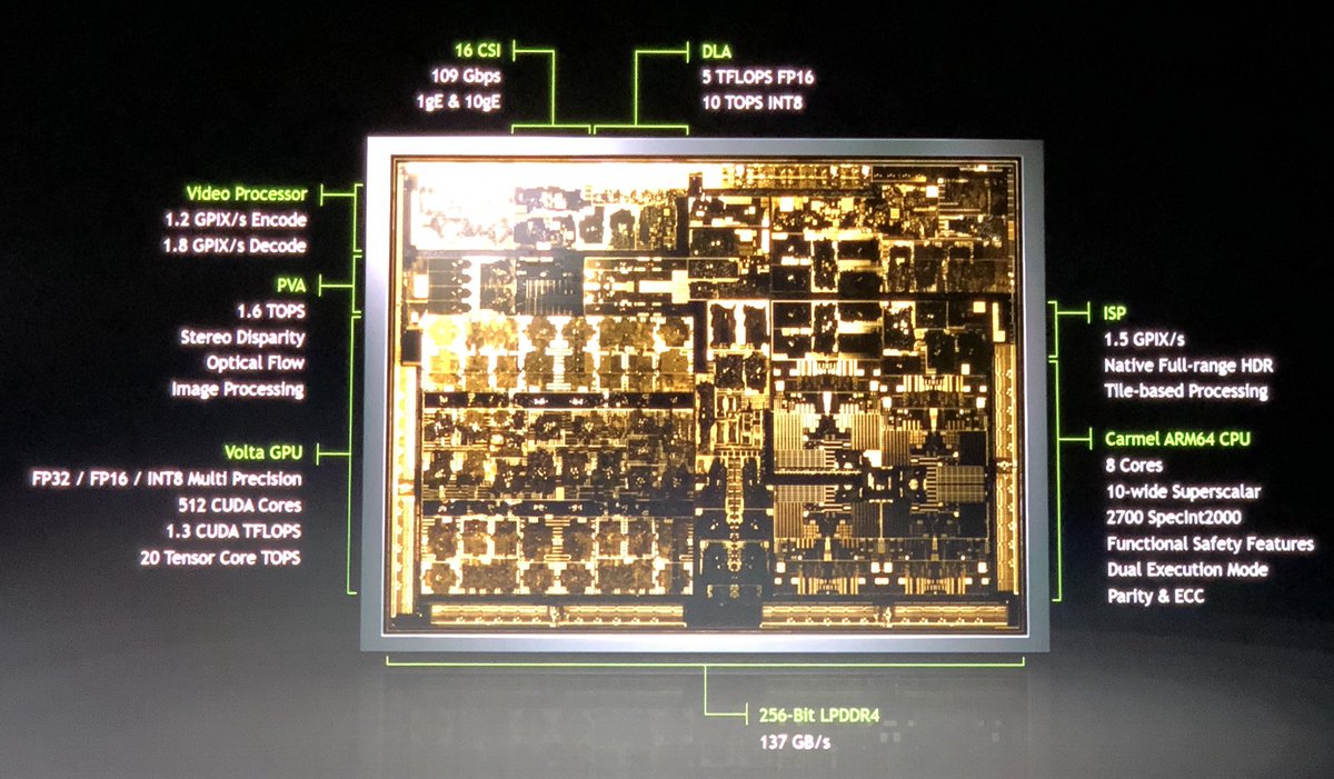
Announced at CES as part of their self-driving car SoC.

10 wide, even wider than Denver...
 

Qwertilot

Golden Member
Nov 28, 2013
1,604
257
126
Not worth it & still tough w'out an x86 license, Q'Com non withstanding. This thing looks at least somewhat specalised for supporting their other computational stuff. Probably very much so.
 

NostaSeronx

Diamond Member
Sep 18, 2011
3,683
1,218
136
9 Billion Transistors, 350mm squared , 12nm FFN... which means when shrinked it will be sub-200 mm squared.

Is that dual execution mode about AArch32/AArch64 or is it something else?

http://s22.q4cdn.com/364334381/files/doc_presentations/2018/01/JHH_CES2018_FINAL_PRESENTED.PDF

TSzhI2k.jpg

Carmel dual-core cluster zoomed.

Also, Zen is a 10-wide architecture based on Nvidia's definition.
Zen: 4 ALUs, 2 AGUs, 4 FPUs = 10-wide
Denver: 1 JSR, 2 IEUs, 2 FPUs, 2 LSUs => 7-wide
Carmel: 1 JSR, 4 IEUs, 3 FPUs, 2 LSUs => 10-wide ((This is a seronx estimate)) // (edit: 3 IEU, 3 FPU, 3 LSU, 1 JSR is more likely the longer I look at it.))

Guessing: 512 KB L2 cache?, Two 256 KB L1Ds?, Two 64 KB L1is? (L2 could be 1 MB, but that is super dense..)

L2 is the bottom unit or top(flip the image), then there is the L1Ds, L1is, and initial branch prediction/fetch logic. The integer registers are right next to the L1is, the FPU registers on the exact top, with the FPU units being around it. The FPU front-ends is in between the FPU registers, not next to the Integer schedulers, etc.
 
Last edited:

NTMBK

Lifer
Nov 14, 2011
10,208
4,940
136
So why nVIDIA doesn't dare to enter to the laptop market?

They got burned once before with Windows RT, remember?

Anyway, NVidia don't currently make any SoCs suitable for laptops or tablets. They used to make tablet SoCs, but all their latest ones are more focused on automotive.
 

Nothingness

Platinum Member
Jul 3, 2013
2,371
713
136
Anyway, NVidia don't currently make any SoCs suitable for laptops or tablets. They used to make tablet SoCs, but all their latest ones are more focused on automotive.
You mean except for the Tegra X1 used in the Nintendo Switch?
 
  • Like
Reactions: killster1

NTMBK

Lifer
Nov 14, 2011
10,208
4,940
136
You mean except for the Tegra X1 used in the Nintendo Switch?

The Tegra X1 is the last one that was tablet suitable, and is pretty old now- it's a 20nm SoC in a 10nm world. They announced it three years ago!
 

dark zero

Platinum Member
Jun 2, 2015
2,655
138
106
They got burned once before with Windows RT, remember?

Anyway, NVidia don't currently make any SoCs suitable for laptops or tablets. They used to make tablet SoCs, but all their latest ones are more focused on automotive.
But now they have a real promise with Parker and Xavier!
And those SoCs now fits perfectly on Laptops.
Finally Microsoft would be pleased to add more ARM manufacturers to maintain their domain.
 

Jan Olšan

Senior member
Jan 12, 2017
273
276
136
Do we know if this is another transmeta design like denver?

They used the same terminology "x-issue superscalar" for Denver, so I would say the architecture principle is the same, still Transmeta.

is it wider than skylake and zen?
Zen has a 6-wide front end, and 8-wide retire.
I don't think you can compare them if Nvidia still uses the VLIW architecture with runtime JIT in software.
The original Denver was also caleld "7-issue superscalar", and it wasn't a tremendously strong core.

project_denver_prvni_detaily_03.png


Speaking of Denver: https://twitter.com/FioraAeterna/status/855445075341398017 :)
 

NTMBK

Lifer
Nov 14, 2011
10,208
4,940
136
They used the same terminology "x-issue superscalar" for Denver, so I would say the architecture principle is the same, still Transmeta.


I don't think you can compare them if Nvidia still uses the VLIW architecture with runtime JIT in software.
The original Denver was also caleld "7-issue superscalar", and it wasn't a tremendously strong core.

project_denver_prvni_detaily_03.png


Speaking of Denver: https://twitter.com/FioraAeterna/status/855445075341398017 :)

Oh wow, that bug is fun!
 

dark zero

Platinum Member
Jun 2, 2015
2,655
138
106
Some Geekbench would be useful there in order to see how it fares against X86 and other ARM processors.
 

Hitman928

Diamond Member
Apr 15, 2012
5,181
7,631
136
Oh wow, that bug is fun!

I'm not really in this space, but I've heard rumblings that the Denver chip was a bug ridden mess. This was just one example that went viral (viral as far as CPU bugs go).
 

Nothingness

Platinum Member
Jul 3, 2013
2,371
713
136
Phoronix have got their hands on one of these, and ran a few quick benchmarks:

embed.php


https://www.phoronix.com/scan.php?page=article&item=nvidia-carmel-quick&num=1

I don't think any of their tests are single threaded, sadly, so tricky to tell how ST performance has scaled.
Yeah, everything is multi-threaded.

Someone posted the same benchmarks with a properly configures Jetson TX2 board: https://openbenchmarking.org/result/1809258-RA-1809248RA57. Read the comments: https://www.phoronix.com/forums/for...quick-test-of-nvidia-s-carmel-cpu-performance

It looks like Phoronix runs the TX2 in default mode where only 4 cores are being used (the Cortex-A57). When the SoC is set to run its 6 cores, then TX2 is faster than Xavier.
 
  • Like
Reactions: dark zero

dark zero

Platinum Member
Jun 2, 2015
2,655
138
106
Yeah, everything is multi-threaded.

Someone posted the same benchmarks with a properly configures Jetson TX2 board: https://openbenchmarking.org/result/1809258-RA-1809248RA57. Read the comments: https://www.phoronix.com/forums/for...quick-test-of-nvidia-s-carmel-cpu-performance

It looks like Phoronix runs the TX2 in default mode where only 4 cores are being used (the Cortex-A57). When the SoC is set to run its 6 cores, then TX2 is faster than Xavier.
Something is telling to me that the Carmel board is not well configured...
 

DrMrLordX

Lifer
Apr 27, 2000
21,582
10,785
136
The Tegra X1 is the last one that was tablet suitable, and is pretty old now- it's a 20nm SoC in a 10nm world. They announced it three years ago!

There's a TX2 now. Nintendo was too cheap to use it in the first run of the Switch. Hopefully they'll come to their senses and use the TX2 in a hardware refresh somewhere down the road. Should extend battery life and/or enable Nintendo to use higher clocks when the console isn't docked.