AMD slide at ISSCC 2017 stated that the 8 MB L3 cache is 19.1 mm2 for Skylake
If this is true the slide I posted is way off. Not sure if I trust AMD numbers though.

AMD slide at ISSCC 2017 stated that the 8 MB L3 cache is 19.1 mm2 for Skylake
And also there are two entries which seems to be Coffee Lake based:
Genuine Intel(R) CPU 0000 @ 3.50GHz (6C 3.5GHz, 6x 256kB L2, 9MB L3)
http://ranker.sisoftware.net/show_r...d5e3dbecdfe6d4f280bd8dabceab96a680f3cef6&l=en
Genuine Intel(R) CPU 0000 @ 3.70GHz (4C 8T 3.7GHz, 4x 256kB L2, 6MB L3)
http://ranker.sisoftware.net/show_r...d5e3d0e2dbe2d7f183be8ea8cda895a583f0cdf5&l=en
Sisoft says it's a Kabylake Client platform but given that Kabylake doesn't support 6C this is more likely a misread. One interesting aspect, Sisoft reports 9MB L3 for the 6C version. It's a 6/6 version which might be Core i5 labeled and Core i7 might get 12 MB then. The 4C version however reports 6MB, so it also could mean Coffee Lake gets 1.5MB L3 per core. Or it's a misread, not sure about that. With only 1.5 MB per core the published Die size from benchlife seems high.
Intel(R) CofeeLake Mobile Graphics Controller
http://ranker.sisoftware.net/show_r...e7d6e3d0e6d4e7c1b38ebe98fd98a595b3c0fdc5&l=en
The descriptions are interesting. 5x8 means 5 subslices of 8 EUs, which is same configuration as Gen 8 and 9. So that does not change.
5x8 = 40EUs, 8 ROPs, 20 TMUs
- 6C/6T Coffee Lake-S model(s) in the works, something I (personally) didn't expect - Intel seems to be taking advantage of the new hexa-core die
And also there are two entries which seems to be Coffee Lake based:
Genuine Intel(R) CPU 0000 @ 3.50GHz (6C 3.5GHz, 6x 256kB L2, 9MB L3)
http://ranker.sisoftware.net/show_r...d5e3dbecdfe6d4f280bd8dabceab96a680f3cef6&l=en
Genuine Intel(R) CPU 0000 @ 3.70GHz (4C 8T 3.7GHz, 4x 256kB L2, 6MB L3)
http://ranker.sisoftware.net/show_r...d5e3d0e2dbe2d7f183be8ea8cda895a583f0cdf5&l=en
Sisoft says it's a Kabylake Client platform but given that Kabylake doesn't support 6C this is more likely a misread. One interesting aspect, Sisoft reports 9MB L3 for the 6C version. It's a 6/6 version which might be Core i5 labeled and Core i7 might get 12 MB then. The 4C version however reports 6MB, so it also could mean Coffee Lake gets 1.5MB L3 per core. Or it's a misread, not sure about that. With only 1.5 MB per core the published Die size from benchlife seems high.
Intel(R) CofeeLake Mobile Graphics Controller
http://ranker.sisoftware.net/show_r...e7d6e3d0e6d4e7c1b38ebe98fd98a595b3c0fdc5&l=en
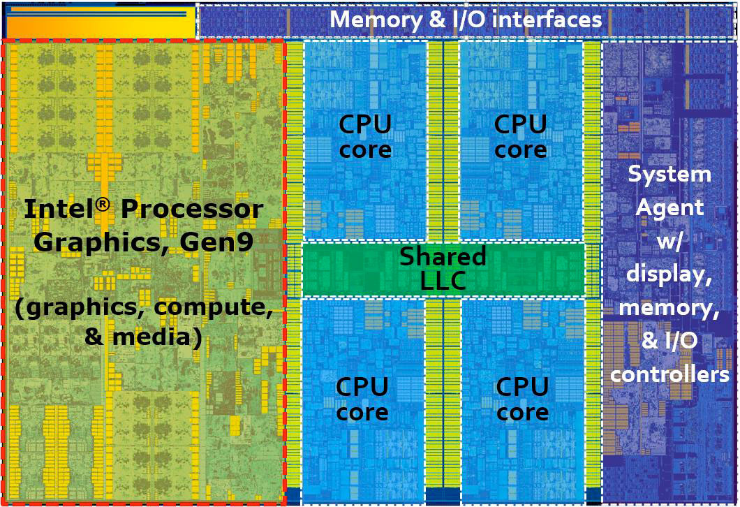
L3 Cache isn't really big: https://www.techpowerup.com/img/15-08-18/77a.jpg
How big is one SKL/KBL core? 10 mm²? 8 MB L3 shouldn't bigger than 5-6 mm², adding 4 MB more L3 would be tiny overall. CFL 6+2 is 149 mm² big according to Benchlife.
AMD slide at ISSCC 2017 stated that the 8 MB L3 cache is 19.1 mm2 for Skylake
If this is true the slide I posted is way off. Not sure if I trust AMD numbers though.
The page also says Gen10 GT2 features two slices.
#define GEN10_FEATURES(_gt, _slices, _l3)
+static const struct gen_device_info gen_device_info_cnl_gt2 = {
+ GEN10_FEATURES(2, 2, 6)
The 4C-8T score is too old to be Coffe Lake based, it says 13 May 2016... but the first one looks to be the real deal.
If the 5x8 description is true though, it excludes the possibility of having it a 2 slice device. Because Gen has subslices 5 doesn't divide into a whole number. Unless it has 5 slices of course.
They'll need something bigger than 149mm^2 if they are to fit 2MB L3/core.
Skylake is 12.25mm^2/core. The difference between 4+2 and 6+2 as posted here is 23 mm^2. That's why.Could you explain why? As I told L3 looks really small in Die shots.
Skylake is 12.25mm^2/core. The difference between 4+2 and 6+2 as posted here is 23 mm^2. That's why.
The first digit doesn't reflect the numbers of subslices in one slice by the looks of it because even for the GT3 and GT4 it wasn't for Cannonlake: https://forums.anandtech.com/thread...-update-vr-zone.2418879/page-10#post-37185583
GT3 is 9x8 and GT4 13x8, they don't have just one slice for sure. The first digit must refer to the total count of subslices.
It still could have 6x8 physically on Die with one subslice being disabled on GT2, this would explain the 48 EUs on Sisoft. If some EUs or one subslice is faulty Intel could still use such a Die.
DigiTimes said:As Intel's new Kaby Lake processors have not stimulated as much demand as expected since their launch in January, the sources are concerned that Intel's new top-end platform for June and new Coffee Lake processors for August may also face weak demand.
DigiTimes said:Sources from motherboard players pointed out that notebooks have been gradually taking demand away from traditional PCs as a result of their better specifications, smaller form factors and cheaper prices.
The die shot points at some really small size for L3 indeed (pixel counting the green area gives me ~5mm2), but I'm left wondering WTH that yellow space around the blu cores and green LLC is then. Unused, dark silicon to cool off the die? But it has patterns and looks like pools of SRAM...
If it is part of the L3 it's easy to understand AMD claim of 19mm2 (I still get a bit less, ~16mm2 but whatever).
Yes, the yellow stuff is the LLC cache arrays. the "green" stuff is just the LLC/ring logic I think.
DIY only:If they mean traditional PCs by Desktops as a proportion of sales, then no. The ratio is same as it was in the early 2000's. Nowadays, increasingly notebooks are replace-every-year $1000+ devices. Yes, there are a category of people that prefer Laptops. I think the proportion would have been greater, but Tablets took most of that away.
Despite some research firms believing that worldwide PC shipments' decline has already started slowing down, many motherboard players still see weak demand from the PC DIY channel, especially in China. As a result, the players believe their motherboard and graphics card shipments in 2017 are unlikely to recover and the overall volume may drop over 10% on year.