ShintaiDK
Lifer
- Apr 22, 2012
- 20,378
- 146
- 106
Again, same old tune, if they made a mainstream hex core, would not have to worry about any of this.
Then people would just complain about 8 and 10 cores and how their hexcore was uncore starved.

Again, same old tune, if they made a mainstream hex core, would not have to worry about any of this.
Server uncore huh. Do the HEDT platforms have the server uncore on their CPUs?
Yes and have for quite a while. They are all currently effectively die chops of the server parts. Though it probably makes sense for them to switch HEDT over to chops of Xeon-D instead of Xeon-E.
Xeon-D is a limited SoC type. It would not fit the HEDT role.
Remember dual channel memory too.
Remember dual channel memory too.
Not to mention a lot of wasted silicon. A lot of the embedded features won't be used by enthusiasts in the HEDT segment.
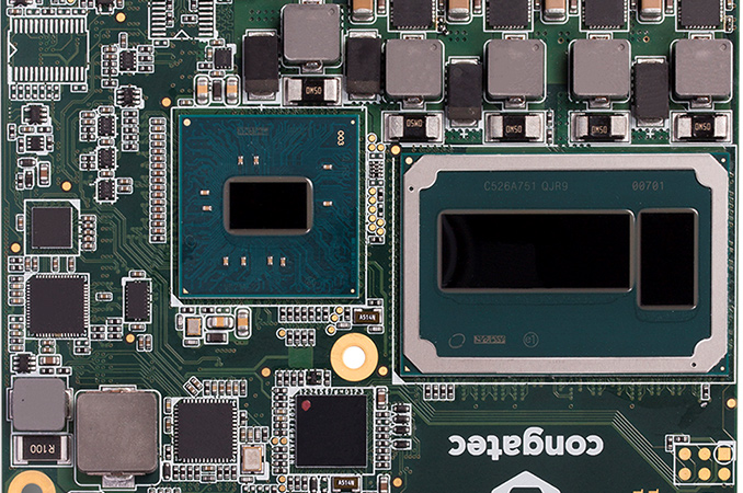
Intel has reportedly updated its price list with three new Skylake-H processors: the Core i7-6785R, the Core i5-6685R, and the Core i5-6585R.
...
")
I hate intel for this..Why they didnt release 6700k with Edram?Or atleast 7700k with edram.
So they can sell Skylake-C when it comes out.
Then they should bloody well come out with it already.
They have to sell Skylake-K first. But not before Kabylake-K.
Considering how much trouble they've had with volume, you'd think they could clear out inventory quickly.
Maybe they're worried that they don't have anything else compelling after launching those two products. Except . . . consumer hexcores with eDRAM!
So they can sell Skylake-C when it comes out.
The eDRAM interface is on the long axis. This setup won't fit in LGA1151.
A Skylake-C version is going to need a bigger socket or a new GT2/GT3 die without the hilariously long GPU.
And then maybe 100 people will buy it, so it'll be $100K USD per CPU.
Hell that die is huge, add the eDRAM and selling this SKU for only $370 will have very small margins.
I really like to see how it performs in DX-12 games.
That chip has 72EUs, and its very similar in die size to the 48EU equipped 5775C. On the same process too. So perf/process/mm2 likely went up nearly 50%.
5775C is about 200mm2, and this chip is at ~215mm2 or so. Perhaps the difference is even less, at 10mm2. It opens up the possibility of a 96EU or perhaps 128EU GPU if they want to go all the way to 300mm2.
Now that AMD, Intel and NVIDIA are at very similar process (14/16nm), it will be very informative to see how this 120mm2 14nm Intel iGPU will perform vs AMD and NVIDIA 110-120mm2 Polaris and Pascal.