Discussion Intel Meteor, Arrow, Lunar & Panther Lakes + WCL Discussion Threads

Page 969 - Seeking answers? Join the AnandTech community: where nearly half-a-million members share solutions and discuss the latest tech.

Tigerick

Senior member
Apr 1, 2022
942
857
106
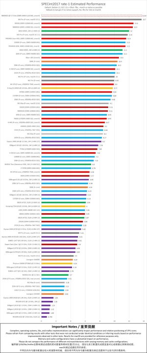
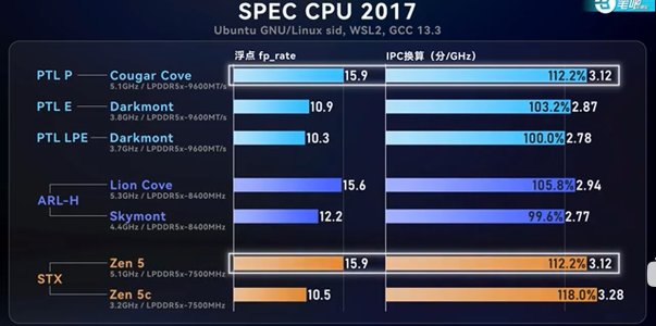
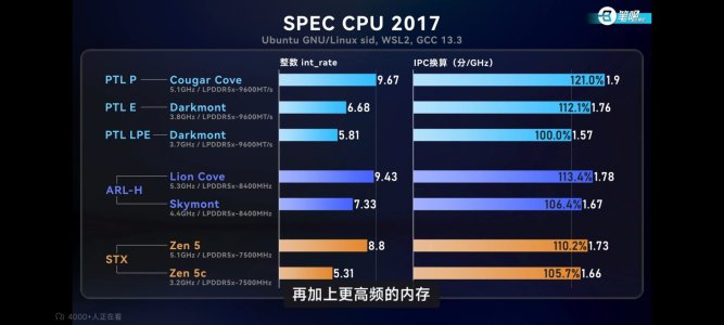
Wildcat Lake (WCL) Specs

Intel Wildcat Lake (WCL) is upcoming mobile SoC replacing Raptor Lake-U. WCL consists of 2 tiles: compute tile and PCD tile. It is true single die consists of CPU, GPU and NPU that is fabbed by 18-A process. Last time I checked, PCD tile is fabbed by TSMC N6 process. They are connected through UCIe, not D2D; a first from Intel. Expecting launching in Q1 2026.

Intel Raptor Lake UIntel Wildcat Lake 15W?Intel Lunar LakeIntel Panther Lake 4+0+4
Launch DateQ1-2024Q2-2026Q3-2024Q1-2026
ModelIntel 150UIntel Core 7Core Ultra 7 268VCore Ultra 7 365
Dies2223
NodeIntel 7 + ?Intel 18-A + TSMC N6TSMC N3B + N6Intel 18-A + Intel 3 + TSMC N6
CPU2 P-core + 8 E-cores2 P-core + 4 LP E-cores4 P-core + 4 LP E-cores4 P-core + 4 LP E-cores
Threads12688
Max Clock5.4 GHz?5 GHz4.8 GHz
L3 Cache12 MB12 MB12 MB
TDP15 - 55 W15 W ?17 - 37 W25 - 55 W
Memory128-bit LPDDR5-520064-bit LPDDR5128-bit LPDDR5x-8533128-bit LPDDR5x-7467
Size96 GB32 GB128 GB
Bandwidth136 GB/s
GPUIntel GraphicsIntel GraphicsArc 140VIntel Graphics
RTNoNoYESYES
EU / Xe96 EU2 Xe8 Xe4 Xe
Max Clock1.3 GHz?2 GHz2.5 GHz
NPUGNA 3.018 TOPS48 TOPS49 TOPS


PPT1.jpg
PPT2.jpg
PPT3.jpg


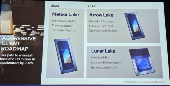
As Hot Chips 34 starting this week, Intel will unveil technical information of upcoming Meteor Lake (MTL) and Arrow Lake (ARL), new generation platform after Raptor Lake. Both MTL and ARL represent new direction which Intel will move to multiple chiplets and combine as one SoC platform.

MTL also represents new compute tile that based on Intel 4 process which is based on EUV lithography, a first from Intel. Intel expects to ship MTL mobile SoC in 2023.

ARL will come after MTL so Intel should be shipping it in 2024, that is what Intel roadmap is telling us. ARL compute tile will be manufactured by Intel 20A process, a first from Intel to use GAA transistors called RibbonFET.


LNL-MX.png
 

Attachments

  • PantherLake.png
    PantherLake.png
    283.5 KB · Views: 24,044
  • LNL.png
    LNL.png
    881.8 KB · Views: 25,531
  • INTEL-CORE-100-ULTRA-METEOR-LAKE-OFFCIAL-SLIDE-2.jpg
    INTEL-CORE-100-ULTRA-METEOR-LAKE-OFFCIAL-SLIDE-2.jpg
    181.4 KB · Views: 72,439
  • Clockspeed.png
    Clockspeed.png
    611.8 KB · Views: 72,326
Last edited:

DavidC1

Platinum Member
Dec 29, 2023
2,178
3,328
106
  • Like
Reactions: ashFTW

DavidC1

Platinum Member
Dec 29, 2023
2,178
3,328
106
Trip down memory lane...

The Pentium back end.
U and V INT pipes and A FP pipe. No scheduler, no OoO but those clever engineers came up with a "controller" to send a pair of instructions in program order down the U pipe to be executed at the same time... boom! Superscaler with no OoO!
The U and V pipe config is still used today. That's why the decoders are referred to as 4-1-1-1 or something like that. It means the first decoder is "complex" and can decode instructions that can split up into 4 uops, and the other ones can do 1 and has to send them to the slow as molasses microcode. This is likely to reduce complexity.

The x86 world's advancements largely resolve around trying to solve the decode issue. Clustered decode is likely that solution. Note, it isn't that big of an issue today. Look at how much that section takes, it's a fraction of maybe 20% and ARM does decoding too, just not variable length decode.
K7 ended up better, but it had flaws like the "glued" ALU/AGU blocks and its L2 cache. But its L1 cache was large and low latency so I have to disagree it was due to core design. As for as .18u, AMd did OK with it. It was its crappy SSE performance that probably hurt it more. I would sooner say their iniital .13u process (T-bred A) that sucked.
Actually L1 is extremely close to the core and affects things like how you layout the core and such:
L1 is fundamentally different from the other levels:
-In Atom based uarchs, the instruction boundary is stored in the L1 Instruction cache
-They are separated into Instruction and Data
-The Load and Store performance related to the core directly affects L1 cache throughput
-The fetched instructions are stored in the L1 caches, so are the decoded ones.

When K7 came out sites reported it had an advantage over P3 even in IO throughput, and it also had a fully pipelined FP unit when P3 didn't. The predecessor struggled to clock and Intel had an advantage but K7 just passed by, meaning everything improved including circuitry not just uarch. P3 being based on an older uarch is also proven by how Tualatin topped out at 1.4GHz, while Pentium M pushed all the way to 1.8GHz, despite also having a low power focus.
 
Last edited:

Josh128

Golden Member
Oct 14, 2022
1,536
2,290
106
18A I think only needs to be competitive with N2 for Intel to really stay in the game. Let me put some numbers to what I'm thinking.
If Zen 6 does indeed hit 6.4GHz on a single core and Nova Lake is stuck at 5.7GHz ST then that is not competitive.
Or if Zen 6 is hitting 65,000 in CB R23 at 200W and Nova Lake requires 275W then that is not competitive.
They need to be around 5% in the important metrics.

Now things get "fuzzy" with process and architecture because they are inexorably intertwined. A really great architecture can "cover" for a not so good node, and vice-versa. If 18A has great density and they can get all of those core crammed into a cost effective tile then Nova Lake can do well MT based on just having a transistor advantage.

Max ST frequency, max MT frequency/power/heat, ST IPC, lots of unknowns still. AMD has been firing on all cylinders since they moved to TMSC because for the first time they had the process advantage, which Intel has relied on previously. AMD really only has one ball in the air, architecture, TMSC handles the other one for them. Intel has two balls in the air. It can be a great show IF you don't drop a ball.

I think Panther Lake is looking to be a rather big technical success for Intel. 5.1GHz on 18A ain't bad for mobile. Efficiency looks to be very good if not great. iGPU is very, very good with no reports (so far) of major driver issues (Alchemist R&D paying dividends), and CPU performance did creep ahead of Lion Cove, which has the advantage of being desktop in terms of memory subsystem.

If they can get the clocks competitive with Zen 6 (whatever that will be) and pull another 5% out of Cougar Cove and catch up in gaming this could be fun. Yeah I know, lots of "ifs."
Clocks dont need to be competitive with Zen 6 if IPC increases another 10% from Panther Lake. Vs Zen 5, Panther Lake is already +10% ahead in integer IPC and tied in fp IPC. They pull off a +10/+10 in Nova Lake and they can afford to be down 10% in clocks and still be competitive.
 

Hulk

Diamond Member
Oct 9, 1999
5,380
4,095
136
Clocks dont need to be competitive with Zen 6 if IPC increases another 10% from Panther Lake. Vs Zen 5, Panther Lake is already +10% ahead in integer IPC and tied in fp IPC. They pull off a +10/+10 in Nova Lake and they can afford to be down 10% in clocks and still be competitive.
Let's unpack this.
I think you are referring to the SPEC 2017 results?
They showed Cougar Cove +10% over Zen 5 for INT and even for FP.

I wonder how that +10% INT and 0% FP will translate into applications and benchmarks we know and love? I wish we have an apples-to-apples comparison of Cougar Cove and Lion Cove to get a little more perspective.

Let's say Zen 6 is 5% behind Coyote Cove. That means Nova could stand a 5% regression in frequency compared to Zen 6. That would be like 6.3GHz for Zen 6 and 6GHz for Coyote Cove.

That's a possible situation. But a worst case for Intel would be Zen 6 shows +5% IPC and frequency over Coyote Cove. That is possible as well. As I've been saying all of this silence from AMD might indicate a quiet confidence. You know how you don't have to talk it up when you have the goods?

If I had to put money on it we'll be seeing another neck-to-neck race at the top of the stack.
 

Hulk

Diamond Member
Oct 9, 1999
5,380
4,095
136
The U and V pipe config is still used today. That's why the decoders are referred to as 4-1-1-1 or something like that. It means the first decoder is "complex" and can decode instructions that can split up into 4 uops, and the other ones can do 1 and has to send them to the slow as molasses microcode. This is likely to reduce complexity.
But isn't the difference that P5's U/V pipes must retain program instruction order? I mean for the change in terminology. When OoO scheduling become possible with P6 Intel abandoned the U/V nomenclature and moved to execution ports and execution units to describe the back end.

For example, Broadwell was 3+1, 3 simple and 1 complex decoder so it was referred to as "4 wide." It could either decode 4 uops/cycle using the legacy decoders or pull 4 uops/cycle from the uop cache via Loop Stream Detector (LSD). Either way 4 wide.

But then with Skylake Intel is calling it "5 wide" even though the decoders are still 3+1. But, the bandwidth of the uop cache was increased to 6 uops. I have been under the impression (probably totally wrong!) that they got "5" as an average of 4 from the legacy decoders and 6 from the uop cache for an average of 5. Or is there some case where the complex decoder can fuse two uops into one or something clever like that going on that changed from Broadwell to Skylake? The only thing I'm seeing different in the back end that would make Skylake wider than Broadwell is the 6uops/cycle uop cache bandwidth increase.

This has been something I've never quite understood fully.
 

reaperrr3

Member
May 31, 2024
176
505
96
Clocks dont need to be competitive with Zen 6 if IPC increases another 10% from Panther Lake. Vs Zen 5, Panther Lake is already +10% ahead in integer IPC and tied in fp IPC. They pull off a +10/+10 in Nova Lake and they can afford to be down 10% in clocks and still be competitive.
I'm 99% positive boosting integer IPC was the focus of Zen6 and will be where most of the 10%+ IPC increase will be coming from.

MLID says that according to one of his sources (yeah yeah, I know, it's MLID, but at least for Zen IPC leaks his track record is decent enough) that FP IPC will only increase by about ~6%, yet the (proven to be legit) core roadmap slide leak clearly stated 10%+ in total IPC increase, so I'd wager AMD aimed for over 10% INT IPC increase.

Zen5 massively boosted FP, especially the PRF which was flat out doubled over Zen4, while int only got a measly 16 extra PRF entries despite 50% more ALUs.
adroc mentioned the IntPRF is a bottleneck now, but that also means notably increasing the IntPRF in Zen6 is a low-hanging fruit that may yield fairly big gains.

Anyway, let's say +6% in FP and +14% in INT for an average of +10%, that would put Zen6 ~5% ahead of PTL in average IPC.
If NVL only added 10% over PTL in both, the IPC advantage would be only like 5% over Zen6. It'll need more than that to make up for a 700 MHz deficit.

And don't forget: Higher IPC in specific workload types is not the same as clockspeed.
10% higher clocks are almost guaranteed to uplift perf more uniformly than 10% "higher IPC", which is actually fairly workload-dependant.

Last but not least, I'm still not convinced that Zen6 will top out at only 6.4 GHz. I consider that a conservative assumption, given it's a jump from N4P to N2P. The combined electrical improvements TSMC lists for N3E/P and N2P are decidedly bigger than the improvement from N7P to N5P was, and Zen4 jumped 800 MHz in max clock.
And no, the increased core count per CCD won't have much of an impact on that imo, because if I were AMD, I'd rather keep the base clock / all-core turbo modest to leave enough headroom for high 1C/2C turbo clocks.
 
  • Like
Reactions: Tlh97 and Hulk

regen1

Senior member
Aug 28, 2025
362
455
96

DavidC1

Platinum Member
Dec 29, 2023
2,178
3,328
106
For example, Broadwell was 3+1, 3 simple and 1 complex decoder so it was referred to as "4 wide." It could either decode 4 uops/cycle using the legacy decoders or pull 4 uops/cycle from the uop cache via Loop Stream Detector (LSD). Either way 4 wide.
Yea but Skylake only had 4 physical decoders.
For example, Broadwell was 3+1, 3 simple and 1 complex decoder so it was referred to as "4 wide." It could either decode 4 uops/cycle using the legacy decoders or pull 4 uops/cycle from the uop cache via Loop Stream Detector (LSD). Either way 4 wide.
It can actually to 4+1+1+1, meaning 7 total. And all SIMD since Sandy Bridge or something could be decoded in all of the decoders. 4-wide means it can do 4 simultaneously. The numbers indicate how complex of an instruction it can handle, not throughput. So the first decoder can handle instructions that decode to 4 micro ops, and the rest can only handle that decode to 1 micro op, but you can use all at the same time. The case where it decodes into more than 1 micro op isn't common that's why it's just called 4-wide.

So,
4 = 1-wide
4+1 = 2-wide
4+1+1 = 3-wide
4+1+1+1 = 4-wide
But then with Skylake Intel is calling it "5 wide" even though the decoders are still 3+1. But, the bandwidth of the uop cache was increased to 6 uops. I have been under the impression (probably totally wrong!) that they got "5" as an average of 4 from the legacy decoders and 6 from the uop cache for an average of 5.
It's just what I call "technimarketing". Sounds genuine but tainted by marketing team.
I'm 99% positive boosting integer IPC was the focus of Zen6 and will be where most of the 10%+ IPC increase will be coming from.

MLID says that according to one of his sources (yeah yeah, I know, it's MLID, but at least for Zen IPC leaks his track record is decent enough) that FP IPC will only increase by about ~6%, yet the (proven to be legit) core roadmap slide leak clearly stated 10%+ in total IPC increase, so I'd wager AMD aimed for over 10% INT IPC increase.
"Integer" basically means overall uarch, so if you aim x % for Integer, you'll get that in everything, meaning in AI, in Integer, in FP, whatever you throw at it. Integer is the hardest part to get. FP has roots in accelerators and can be boosted further by other means, and often gets greater gains from additions that are meant for Integer workloads.
 
Last edited:

DrMrLordX

Lifer
Apr 27, 2000
23,217
13,300
136
Clocks dont need to be competitive with Zen 6 if IPC increases another 10% from Panther Lake. Vs Zen 5, Panther Lake is already +10% ahead in integer IPC and tied in fp IPC. They pull off a +10/+10 in Nova Lake and they can afford to be down 10% in clocks and still be competitive.
Isn't Nova Lake also using Cougar Cove?
 

511

Diamond Member
Jul 12, 2024
5,441
4,867
106
No, Novalake is Panther Cove or Cougar Cove with the E core being Arctic Wolf. @511 knows the P core name better.
I thought Panther Cove was just the old name for Cougar Cove before Intel changed it . . .
It's a mess of naming but Panther Cove is the core in diamond rapids and coyote cove is the client version of Panther Cove.

E cores is arctic wolf.

Both are proper Tock
 
  • Like
Reactions: pcp7

511

Diamond Member
Jul 12, 2024
5,441
4,867
106
Not sure if those cores can reach 6GHz+ which is important for desktop on 18A
This is 18AP but I doubt they will doing 6 GHz these are used to make 256C SKU also 48Cores in nova composed of 2 8+16 Tiles same as ARL it's not a single 16+32 die.
Maybe they can make the do 5.5 we will know though cause the 4+0+4 SKU is 18AP
 
  • Like
Reactions: Tlh97 and poke01

DavidC1

Platinum Member
Dec 29, 2023
2,178
3,328
106
Zen5 is a 6k entry macro-OP cache.
Each entry is 1-4 fused ops iirc.
And it's on N4, while P4 is on 0.18u.

The 12Kuops on Willamette is 80-100KB in size. An absolute monster since it's core stuff. It would be considered big today for a uop cache.

I think Intel "wasted" lot of good engineers on the P4. Many fantastic stuff, driven by wrong ideals. Also while @igor_kavinski wants 18A Pentium 4, I'd like everything in Prescott WITHOUT the 31 stage pipeline, stay at 20 like the predecessor. 20-30% extra perf/clock would have made things look a lot different.
 

Abwx

Lifer
Apr 2, 2011
12,012
4,973
136
Let's unpack this.
I think you are referring to the SPEC 2017 results?
They showed Cougar Cove +10% over Zen 5 for INT and even for FP.
In spec int the 358H with 8533 RAM is at the same level as a cut down cache KRK AI 350 using 5600 RAM, what about if RAM speeds where the same, so from where did you pull those 10%.?.

As for FP is your reference Cinebench.?.
Because in all other renderers Zen 5 has better ST IPC than the 285K.

Edit : At 5.1 GHz the 9950X would do 11.27, that s 9.4% better than the 358H, seems
that you got your numbers completely inverted.
 

Attachments

  • HAATgu8bAAA6LYX.jpg
    HAATgu8bAAA6LYX.jpg
    346.6 KB · Views: 21
Last edited:

Hulk

Diamond Member
Oct 9, 1999
5,380
4,095
136
In spec int the 358H with 8533 RAM is at the same level as a cut down cache KRK AI 350 using 5600 RAM, what about if RAM speeds where the same, so from where did you pull those 10%.?.

As for FP is your reference Cinebench.?.
Because in all other renderers Zen 5 has better ST IPC than the 285K.
I pulled them from these, which are in this thread.
Also, Lion Cove seems to be a little better than Zen 5 in CB.
1770211976757.png
 

Attachments

  • SPEC 2017 FP.jpg
    SPEC 2017 FP.jpg
    278.5 KB · Views: 12
  • SPEC 2017 INT.jpeg
    SPEC 2017 INT.jpeg
    92.5 KB · Views: 16

Abwx

Lifer
Apr 2, 2011
12,012
4,973
136
I pulled them from these, which are in this thread.
Also, Lion Cove seems to be a little better than Zen 5 in CB.
View attachment 137877
I edited my previous post, at 5.1GHz the 9950X would be 9.4% faster than the 358H in Spec, beside Cinebench is an exception, it s the olny renderer where intel has better ST than Zen 5, in all other renderers without exception Zen 5 has better ST IPC, so that s just cherry picking what is most favourable to Intel while ignoring scores of other tests.

Edit : The 358H is only 4.8GHz, so that s only 3% better in Spec for the 9950X clock/clock, but the former has much faster RAM, 52%, to begin with.
 
Last edited:

Hulk

Diamond Member
Oct 9, 1999
5,380
4,095
136
I edited my previous post, at 5.1GHz the 9950X would be 9.4% faster than the 358H in Spec, beside Cinebench is an exception, it s the olny renderer where intel has better ST than Zen 5, in all other renderers without exception Zen 5 has better ST IPC, so that s just cherry picking what is most favourable to Intel while ignoring scores of other tests.

Edit : The 358H is only 4.8GHz, so that s only 3% better in Spec for the 9950X clock/clock, but the former has much faster RAM, 52%, to begin with.
I have no dog in this hunt!
I'm all for Intel and AMD.

Good points!