Discussion Intel Meteor, Arrow, Lunar & Panther Lakes Discussion Threads

Page 841 - Seeking answers? Join the AnandTech community: where nearly half-a-million members share solutions and discuss the latest tech.

Tigerick

Senior member
Apr 1, 2022
789
757
106
PPT1.jpg
PPT2.jpg
PPT3.jpg


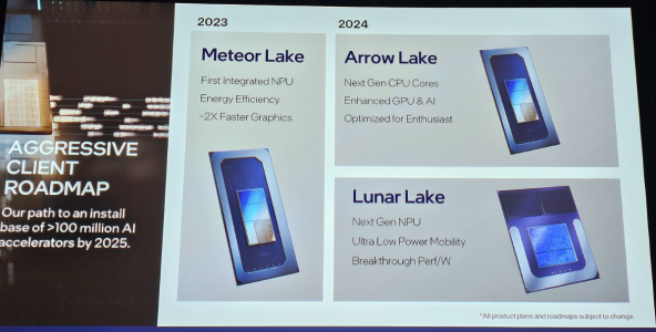
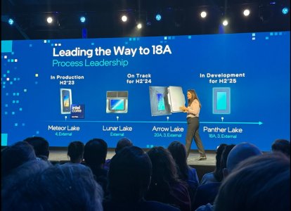
As Hot Chips 34 starting this week, Intel will unveil technical information of upcoming Meteor Lake (MTL) and Arrow Lake (ARL), new generation platform after Raptor Lake. Both MTL and ARL represent new direction which Intel will move to multiple chiplets and combine as one SoC platform.

MTL also represents new compute tile that based on Intel 4 process which is based on EUV lithography, a first from Intel. Intel expects to ship MTL mobile SoC in 2023.

ARL will come after MTL so Intel should be shipping it in 2024, that is what Intel roadmap is telling us. ARL compute tile will be manufactured by Intel 20A process, a first from Intel to use GAA transistors called RibbonFET.


LNL-MX.png

Intel Core Ultra 100 - Meteor Lake

INTEL-CORE-100-ULTRA-METEOR-LAKE-OFFCIAL-SLIDE-2.jpg

As mentioned by Tomshardware, TSMC will manufacture the I/O, SoC, and GPU tiles. That means Intel will manufacture only the CPU and Foveros tiles. (Notably, Intel calls the I/O tile an 'I/O Expander,' hence the IOE moniker.)


Clockspeed.png
 

Attachments

  • PantherLake.png
    PantherLake.png
    283.5 KB · Views: 24,025
  • LNL.png
    LNL.png
    881.8 KB · Views: 25,517
Last edited:

Fjodor2001

Diamond Member
Feb 6, 2010
4,162
569
126
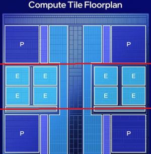
if you cut that 4+8 in half ut becomes 4+0/8+0.
I suppose you mean it becomes 4+0/0+8?

But is it really possible to cut it like that and still get usable dies. I added some red lines in the picture. Do you mean it should be cut along those red lines, or some other way?

1754812382035.png

The 4 P cores would be on two separate dies after the cutting then. :confused:

Wouldn't cutting it in the middle to get two 2+4 dies be a more logical option instead?
 

511

Diamond Member
Jul 12, 2024
3,449
3,330
106
I suppose you mean it becomes 4+0/0+8?

But is it really possible to cut it like that and still get usable dies. I added some red lines in the picture. Do you mean it should be cut along those red lines, or some other way?

View attachment 128536

The 4 P cores would be on two separate dies after the cutting then. :confused:

Wouldn't cutting it in the middle to get two 2+4 dies be a more logical option instead?
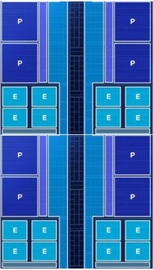
So the layout is a bit changed 2P Cores Shares a L2 Slice and also this is how i expect NVL Die Layout
1754813837535.png
 

DKR

Junior Member
Nov 19, 2024
10
15
41
IDK about SKU but the plan to make 4+8 using 18AP is canned it is using TSMC N2 now
Are you 100% confident about this? Because they already have a 4P+8E die on 18A for PTL-H? so it shouldn't be a big deal do that in 18A-P to do the same considering its just a related + node. At least what is what I thought. Also NVL is already taped out by the time Foundry direct connect 2025 event & shortly afterwards semiaccurate reported NVL SKUs on N2 taped out, I highly doubt Lip Bu Tan could have changed something on NVL by then.

Just from engineering POV to reduce engineering effort, to leverage tile arch & benefit from it, it makes sense to do one 8P+16E die on N2P & one 4P+8E die on 18A/18A-P. Then they can mix and match to create SKUs & down bin the 4+8 die to 4+4 & 4+0.
Note if 4+8 die is on 18A/18A-P, the entire mobile line up on NVL- H will be IFS (like PTL-H but on 18A-P), only the NVL-HX (8+16) will be on TSMC. I think this is very important for Intel to regain their margins. So it just baffles me that 4+8 would be on TSMC & that decision being made Lip Bu doesn't sound right with me. He is looking to be bean counter when it comes margins based on recent news about new product being approved only if margin >50%. Intel can't afford to keep outsourcing their products and maintain upkeep of their foundries which are fixed cost business.

This aligns with past commentaries from Pat & Michelle also that NVL is predominantly IFS based (Pat quoted >80% iirc) and only one top end SKU is on TSMC node. Also why MLID is keeping the 4+8 SKU as "high confidence" color instead of "very high confident" color. He is intentionally downplaying 18A-P imho.

I think Intel is only sourcing the 8P+16E bLLC die from TSMC. With that they can make a 2(8P+16E bLLC)+4LPE SKU for a Core Ultra 9, (8P+16E bLLC & 4P+8E[18A-P])+4LPE SKU for Core Ultra 7 & (8P+16E bLLC)+ 4LE for Core Ultra 5 that covers all the gaming crowd requirements of a bLLC SKU to compete with x3D. All these will be K SKUs. All the rest of the main stream K & non K SKUs will be based on 18A-P tiles like 2(4+8)+4LPE, 4+8+4LPE, 4+0+4LPE. This way they limit the outsourcing to TSMC to the minimum. This is just speculation on my part but who knows what is really going on at Intel now!
 
  • Like
Reactions: OneEng2

511

Diamond Member
Jul 12, 2024
3,449
3,330
106
Are you 100% confident about this? Because they already have a 4P+8E die on 18A for PTL-H? so it shouldn't be a big deal do that in 18A-P to do the same considering its just a related + node. At least what is what I thought. Also NVL is already taped out by the time Foundry direct connect 2025 event & shortly afterwards semiaccurate reported NVL SKUs on N2 taped out, I highly doubt Lip Bu Tan could have changed something on NVL by then.
Yes 100%
 
  • Wow
Reactions: DKR

511

Diamond Member
Jul 12, 2024
3,449
3,330
106
Why are people making out about ~30mm2 extra die as bad defect rate its still < 150mm2 not a reticle size die also as DavidC1 said Cache aka SRAM can be worked around for bad yield using redundancy
 
  • Like
Reactions: DKR

511

Diamond Member
Jul 12, 2024
3,449
3,330
106
this is the probable future for intel/usf, keep top-end chips on TSMC latest nodes and keep less performing on their overpromising underdelivering intel nodes
Well at least they can do that what can any other company do? 🤣.
They can change plan based on Internal/External nodes what can other Fabless do pay 10%-20% more.
 

511

Diamond Member
Jul 12, 2024
3,449
3,330
106
Wow, that's worse than I expected...

Well, goodbye Intel Foundries. You had a good run. Don't worry, Intel Product will be following you pretty soon...
LoL you know that there is no NVL without IFS/18A/Intel 3/18AP?
 

Magio

Member
May 13, 2024
140
152
76
LoL you know that there is no NVL without IFS/18A/Intel 3/18AP?

Compute tiles are the most important barometer and the fact there'll only be one of them made on 18A for NVL is a terrible sign. And combined with all the other bad omens including the CEO outright saying they're considering canning 14A... Yeah Intel Foundry's on its way out.
 

511

Diamond Member
Jul 12, 2024
3,449
3,330
106
Compute tiles are the most important barometer and the fact there'll only be one of them made on 18A for NVL is a terrible sign. And combined with all the other bad omens including the CEO outright saying they're considering canning 14A... Yeah Intel Foundry's on its way out.
CEO was talking about financial viability of 14A not technical viability. Their issue is more financial than technical maybe it is due to the CAPEX cut he is doing
 

511

Diamond Member
Jul 12, 2024
3,449
3,330
106
They are a large % of the die. Lithography flaws in cache can still disable a die.
so for example let's say 100mm2 is die size for 8+16 non bLLC and 130 is for bLLC it's not a large die size this is still a relatively small die
 

Magio

Member
May 13, 2024
140
152
76
CEO was talking about financial viability of 14A not technical viability. Their issue is more financial than technical maybe it is due to the CAPEX cut he is doing

Doesn't really matter why LBT is considering dropping 14A and cutting-edge node development in general. Just matters that he is.
 

511

Diamond Member
Jul 12, 2024
3,449
3,330
106
Doesn't really matter why LBT is considering dropping 14A and cutting-edge node development in general. Just matters that he is.
LOL
when Intel changes products from 18A/AP to N2 - 18A is sh**
when Intel gives up foundry due to money problem - doesn't matter
 

LightningZ71

Platinum Member
Mar 10, 2017
2,389
3,033
136
The part that should concern is that Intel has chosen the least performance, smallest possible CPU die for 18A only. It would be one thing if this was the very first part they've ever done on 18A, but isn't Panther Lake, which is also supposed to use 18A supposed to have been in full rate production and general sale for a good 6 months+ by that point? Either they have very little confidence that 18A can hit the desktop performance targets they need, or they will be massively capacity constrained and will only make what can get high volume on that in house mode.