Discussion Intel Meteor, Arrow, Lunar & Panther Lakes Discussion Threads

Page 826 - Seeking answers? Join the AnandTech community: where nearly half-a-million members share solutions and discuss the latest tech.

Tigerick

Senior member
Apr 1, 2022
782
750
106
PPT1.jpg
PPT2.jpg
PPT3.jpg


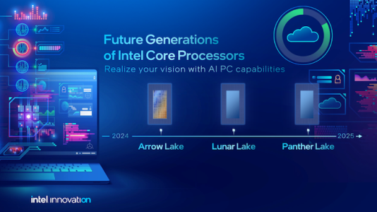
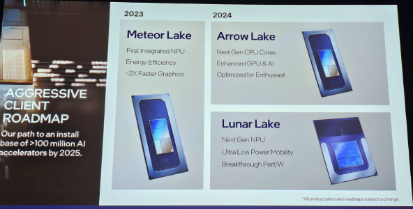
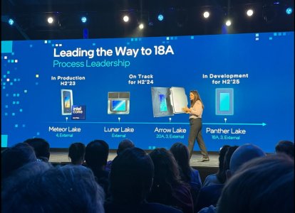
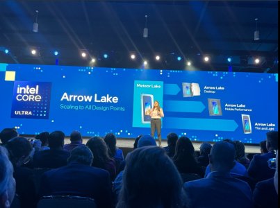
As Hot Chips 34 starting this week, Intel will unveil technical information of upcoming Meteor Lake (MTL) and Arrow Lake (ARL), new generation platform after Raptor Lake. Both MTL and ARL represent new direction which Intel will move to multiple chiplets and combine as one SoC platform.

MTL also represents new compute tile that based on Intel 4 process which is based on EUV lithography, a first from Intel. Intel expects to ship MTL mobile SoC in 2023.

ARL will come after MTL so Intel should be shipping it in 2024, that is what Intel roadmap is telling us. ARL compute tile will be manufactured by Intel 20A process, a first from Intel to use GAA transistors called RibbonFET.


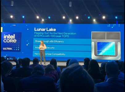
LNL-MX.png

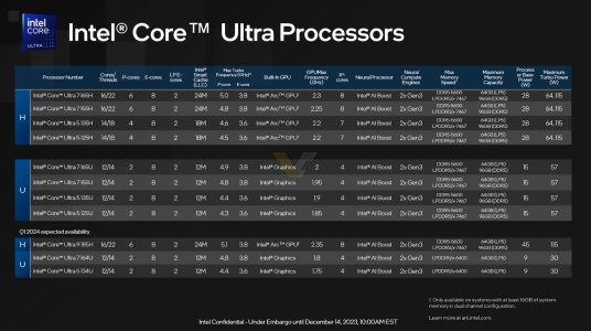
Intel Core Ultra 100 - Meteor Lake

INTEL-CORE-100-ULTRA-METEOR-LAKE-OFFCIAL-SLIDE-2.jpg

As mentioned by Tomshardware, TSMC will manufacture the I/O, SoC, and GPU tiles. That means Intel will manufacture only the CPU and Foveros tiles. (Notably, Intel calls the I/O tile an 'I/O Expander,' hence the IOE moniker.)
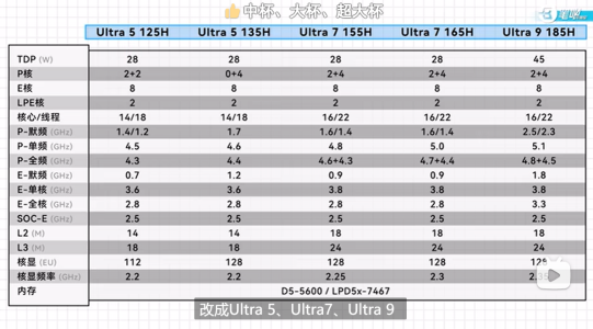


Clockspeed.png
 

Attachments

  • PantherLake.png
    PantherLake.png
    283.5 KB · Views: 24,025
  • LNL.png
    LNL.png
    881.8 KB · Views: 25,517
Last edited:

LightningZ71

Platinum Member
Mar 10, 2017
2,364
2,967
136
The rumor that I've seen for the BLCC die is that they just duplicated the area in the middle of the die where all the L3 already was, making the whole thing wider. I think that they're going to have to make a material improvement in the ring itself to full realize the performance gains of that, though, as there's going to be a lot of constant ring traffic for L3 hits and writes that's going to make an already overstressed design even more heavily stressed. We'll see. I don't think that there will be many places where people will find where it hurts things. The question is more about how much will it really help?
 
  • Like
Reactions: Tlh97 and Geddagod

AcrosTinus

Senior member
Jun 23, 2024
212
219
76
What workloads does your 265K usually crash in? I haven't faced a serious crash on my 245KF yet during normal use but then I haven't used it for 24 hours straight yet. In your case, it seems like possibly a bad sample (could be one reason why they are having a firesale on 265K) or the mobo needs the latest BIOS and try running with only Intel base profile or 200S Boost profile and see if the crashes persist. If they still do, either bad mobo, some other finicky hardware causing the crashes (process of elimination to identify) or finally bad CPU sample.
I assume you encounter no issues because you a) have no IGPU or b) have no MSI board.
  • Visual Studio compiles
  • Handbrake encodes
  • OBS recording via quicksync
  • Docker Desktop containers
  • VMs with VM workstation
  • VMs with Hyper-V
  • Simple Browsing
  • Gaming (Apex, Marvel Rivals)
All these things trigger crashes randomly. Also crashed happen if I do nothing at around 17h it just crashes as well. Also I have used the boost profile, it is buggy as hell and triggers a different set of side effects with the NPU. For now I have gotten a beta BIOS and some voltage settings to apply. The system still crashes though, only using "PEG only" and XMP off provides maximum stability. If I have the time I will troubleshoot more. The 2xU7 and 1xU9 all show the same issues on the MSI board, the ASUS is not affected but has some issues regarding the NPU as well.
 

OneEng2

Senior member
Sep 19, 2022
706
946
106
Just my opinion, but an on-die large L3 is a bad economic idea. Creating a single monolithic large die to get a big L3 is going to decrease yields and increase the wafer waste.

AMD's implementation limits the size of the 3D L3 cache to the size of the original die it is being stacked onto. This is a much better idea for a number of reasons.

Still, Intel will likely achieve the end goal (drastically lowering overall memory latency) using their approach, it will just be expensive for them to do it.

I am not sure how this fits into Intel's desire to increase margins.
 
  • Like
Reactions: Tlh97
Jul 27, 2020
26,328
18,108
146
I assume you encounter no issues because you a) have no IGPU or b) have no MSI board.
Correct. No to both.

I purposely refused to update the drivers. Haven't even checked to see if the NPU driver is installed. I just wanted the vanilla virgin experience (don't laugh).

It was going so well until I hit that stupid RAM OC issue where the Lion Cove cores either don't want to do any work or randomly wake up and work and then stop after about 60 seconds. And 7200 RAM should boot at stock 6400 (Arrow Lake's stock RAM config) but instead resorts to 5600 MT/s. It's pathetic that the memory controller can't figure out if the RAM can run at stock 6400.

I just read this: https://www.xda-developers.com/intel-serious-problem-arrow-lake-memory-compatibility/

I guess I got lucky that I didn't face THAT many RAM problems.
 

coercitiv

Diamond Member
Jan 24, 2014
7,242
17,050
136
Just my opinion, but an on-die large L3 is a bad economic idea. Creating a single monolithic large die to get a big L3 is going to decrease yields and increase the wafer waste.

AMD's implementation limits the size of the 3D L3 cache to the size of the original die it is being stacked onto. This is a much better idea for a number of reasons.
I think the monolithic approach is indeed more expensive to produce, but it's probably less expensive to design... in terms of time to market that is. Intel is still a slow, reactive beast, they're trading cost efficiency for relevance in the consumer market. It will only cost them a few hundred engineer jobs. /s

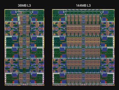
Just for the fun of it, here's a very crude vertical multiplication of the sections that contain L3 on Arrow Lake. It's obviously not accurate, but fast to put together, and puts the big cache die at just under 1.6x the ARL compute die size. Napkin math says this means a more realistic layout estimate would fall under 1.5x area. If the vanilla NVL-S ends up around 95 mm2 then BLLC version would be ~140 mm2.

Playing with cache.jpg
 

Joe NYC

Diamond Member
Jun 26, 2021
3,321
4,857
136
I think the monolithic approach is indeed more expensive to produce, but it's probably less expensive to design... in terms of time to market that is. Intel is still a slow, reactive beast, they're trading cost efficiency for relevance in the consumer market. It will only cost them a few hundred engineer jobs. /s

Just for the fun of it, here's a very crude vertical multiplication of the sections that contain L3 on Arrow Lake. It's obviously not accurate, but fast to put together, and puts the big cache die at just under 1.6x the ARL compute die size. Napkin math says this means a more realistic layout estimate would fall under 1.5x area. If the vanilla NVL-S ends up around 95 mm2 then BLLC version would be ~140 mm2.

View attachment 127657

Then the comparison with Zen 6 + V=Cache would be:
NVL: 140 mm2 N2
Zen 6: 75 mm2 N2 + 75 mm2 N4 or N6
 
  • Like
Reactions: Tlh97 and OneEng2

coercitiv

Diamond Member
Jan 24, 2014
7,242
17,050
136
Then the comparison with Zen 6 + V=Cache would be:
NVL: 140 mm2 N2
Zen 6: 75 mm2 N2 + 75 mm2 N4 or N6
I'm not comfortable comparing rough estimates like this, the figures used for NVL-S were meant to give a sense of scale, not make 1:1 comparisons with Zen 6. I do agree however that AMD is in a position to make the more cost efficient product, at least as far as perf/cost is concerned.
 

LightningZ71

Platinum Member
Mar 10, 2017
2,364
2,967
136
The x factor is the cost of the stacking process, the good dies that they lose in the process, the extra packaging and movement time costs.

I can only guess that cache die yields must be near 100% as there has never even been a mention of a die recovery product for it.
 

gdansk

Diamond Member
Feb 8, 2011
4,297
7,200
136

Just look at this, SMT is coming back and everyone on the 1T per P-Core train have just officially bought a nerfed P-Core CPU, me included.
Note that it is included under the "data center" category. Doesn't say it's coming back to client, where it's of questionable utility when you have e cores to spam.

Personally I'm more interested in what "simplified SKU stacks" will bring than anything else mentioned there.
 

AcrosTinus

Senior member
Jun 23, 2024
212
219
76
Note that it is included under the "data center" category. Doesn't say it's coming back to client, where it's of questionable utility when you have e cores to spam.

Personally I'm more interested in what "simplified SKU stacks" will bring than anything else mentioned there.
I think you can make the inference that it is coming back to client why:
  • The move towards 1T per P-Core was not just in client but also a DC thing.
  • The CEO does not want multiple CPU architectures in development, meaning if SMT is reintroduced with a core family, one can assume that it will will be used across the entire stack, making sure that advancement influence all products.
 

Saylick

Diamond Member
Sep 10, 2012
3,928
9,164
136
I think the monolithic approach is indeed more expensive to produce, but it's probably less expensive to design... in terms of time to market that is. Intel is still a slow, reactive beast, they're trading cost efficiency for relevance in the consumer market. It will only cost them a few hundred engineer jobs. /s

Just for the fun of it, here's a very crude vertical multiplication of the sections that contain L3 on Arrow Lake. It's obviously not accurate, but fast to put together, and puts the big cache die at just under 1.6x the ARL compute die size. Napkin math says this means a more realistic layout estimate would fall under 1.5x area. If the vanilla NVL-S ends up around 95 mm2 then BLLC version would be ~140 mm2.

View attachment 127657
It’s starting to look like a Zen CCD where the cores take up a little under half the total die area lol
 

gdansk

Diamond Member
Feb 8, 2011
4,297
7,200
136
The CEO does not want multiple CPU architectures in development, meaning if SMT is reintroduced with a core family, one can assume that it will will be used across the entire stack, making sure that advancement influence all products.
It might impact unified core, something far off, restoring SMT across all products. But I doubt that.

In either case the cat coves for client do not have SMT validated. Delay and time on rework/retest at this point are unacceptable. I.e. Arrow Lake will not be alone in this regard.
 
  • Like
Reactions: AcrosTinus

reb0rn

Senior member
Dec 31, 2009
305
107
116
SMT is only good for server cloud as they offer clients mostly threads ....so they for them more threads more value
for home users and even for severs maybe best optimization would be without it
 

OneEng2

Senior member
Sep 19, 2022
706
946
106
I'm not comfortable comparing rough estimates like this, the figures used for NVL-S were meant to give a sense of scale, not make 1:1 comparisons with Zen 6. I do agree however that AMD is in a position to make the more cost efficient product, at least as far as perf/cost is concerned.
That is what I am thinking.
SMT is only good for server cloud as they offer clients mostly threads ....so they for them more threads more value
for home users and even for severs maybe best optimization would be without it
While I agree that server benefits the most from SMT, I think that SMT offers the best PPA you can get even in desktop for MT. Getting 40% of a core for 15% die space add is a good deal. This is particularly true because all your cores are identical and don't require you rely on OS scheduling to avoid putting inappropriate loads on processors that can't handle them efficiently ..... or bogging down your P cores with trivial tasks.

I did a comparison of the PPA of Zen 5c vs Skymont (with lots of napkin math) and the were about equal (Skymont was ~10% better using simple math and lots of assumptions). That 10% PPA comes at a pretty big cost though.
 

reb0rn

Senior member
Dec 31, 2009
305
107
116
What I use I never seen more then 10% benefit from SMT... in MT, sure its depend on core but I alone would prefer always real cores
 

511

Diamond Member
Jul 12, 2024
3,191
3,143
106
What I use I never seen more then 10% benefit from SMT... in MT, sure its depend on core but I alone would prefer always real cores
even i did benchmarks on my MTL and in cinebench R23 with and without SMT it was roughly 10-15% difference for 16C/22T vs 16C/16T
 
  • Like
Reactions: reb0rn

511

Diamond Member
Jul 12, 2024
3,191
3,143
106
I need to rebench my setup with 6+8+HT/6+8no HT/6+0/6+0HT.
But the question is what should I bench? Cinebench R23 or 24?
 

reb0rn

Senior member
Dec 31, 2009
305
107
116
I can presume non optimized MT load would benefit from SMT more, while dedicated MT optimized code have almost zero benefit
 

AcrosTinus

Senior member
Jun 23, 2024
212
219
76
If I am less pessimistic, I would call the reintroduction of SMT a positive thing, but somehow my gut tells me, this will be at the cost of ST performance gains because time has to be invested into resurrection and hardening to prevent a SpectreV-X. Time that could have gone into the 1T performance. A super wide P-Core or the so called rumored RU is officially a bed time story.
 

LightningZ71

Platinum Member
Mar 10, 2017
2,364
2,967
136
It very much depends on the code. Completely homogenous tasks will typically run into contention issues as the code streams will fight for the same back end resources. Heterogenous code will better exploit the back end, especially if it is very wide. Low predictability branchy code won't stall the whole core, just one thread. Code that has lower memory demand can better share the caches.
 
  • Like
Reactions: igor_kavinski